Method of driving plasma display panel

a technology of plasma display panel and drive mechanism, which is applied in the direction of instruments, static indicating devices, etc., can solve the problem of reducing the contrast characteristic of pdp according to the related ar

Inactive Publication Date: 2006-03-14
INTELLECTUAL DISCOVERY CO LTD
View PDF5 Cites 34 Cited by
  • Summary
  • Abstract
  • Description
  • Claims
  • Application Information

AI Technical Summary

Benefits of technology

[0057]More preferably, an erase pulse to erase the wall charges remaining on the electrodes in each of the sub-fields is supplied as the pulse to reduce the voltage difference between the scan and sustain electrodes.

Problems solved by technology

However, the PDP according to the related art decreases its contrast characteristic since the wall charges are excessively formed on the scan and sustain electrodes Y and Z during the reset period.

Method used


Image

  • Method of driving plasma display panel
  • Method of driving plasma display panel
  • Method of driving plasma display panel

Examples


first embodiment

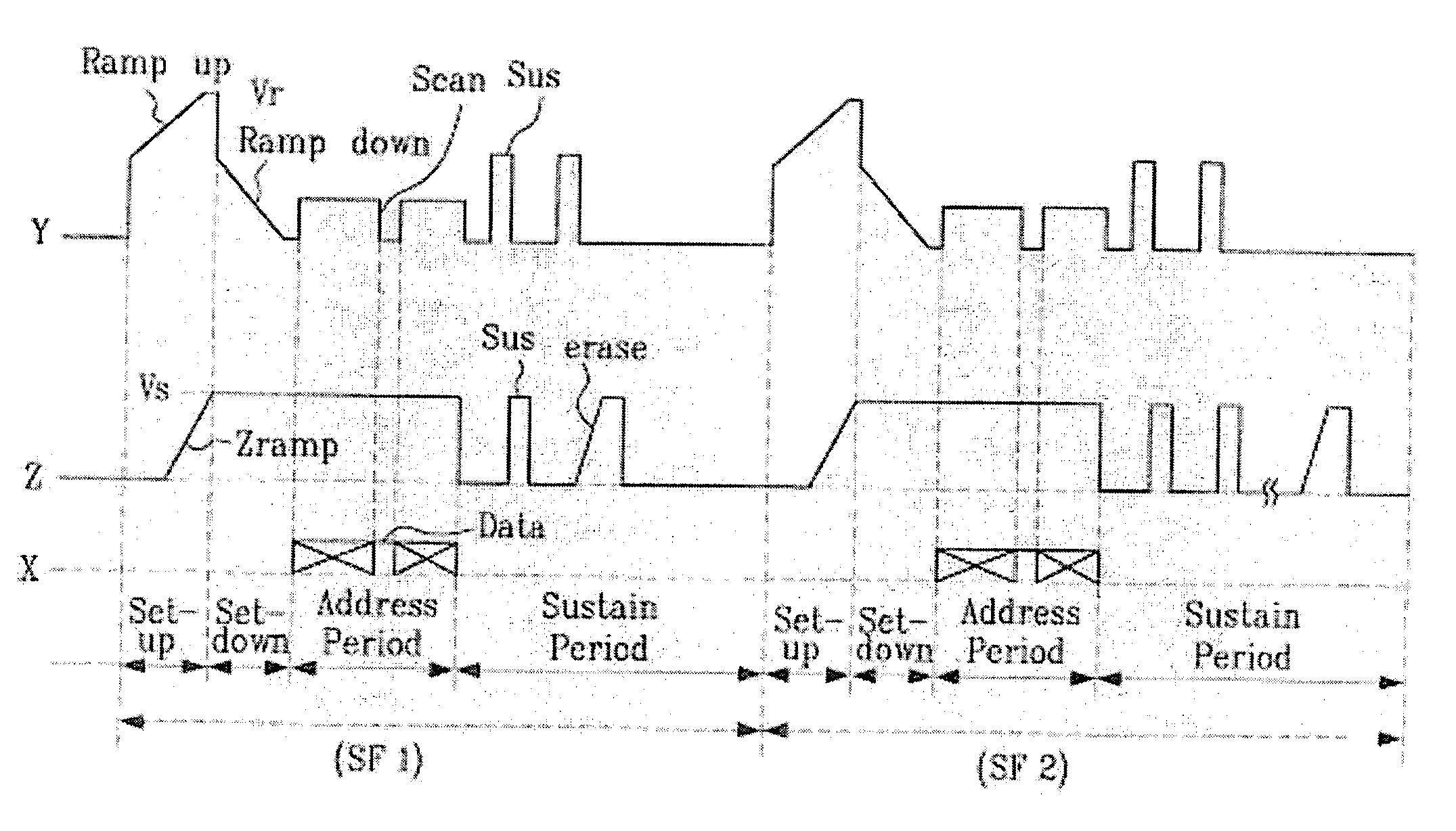
[0103]FIG. 4 illustrates a method of driving a PDP according to the present invention, in which a pulse Zramp of a ramp-up waveform is applied for a set-up period of each sub-field to reduce a voltage difference between scan and sustain electrodes Y and Z.

[0104]Referring to FIG. 4, a first embodiment of the present invention is explained in detail as follows.

[0105]First of all, while a ramp-up reset pulse is applied to a scan electrode Y, a ramp-up pulse Zramp is applied to a sustain electrode Z from a predetermined time point(especially, from the latter period of a set-up period). The ramp-up pulse Zramp ascends to a voltage level Vs of a sustain pulse Sus from a base voltage. Since the ramp up pulse Zramp suppresses a discharge between a scan electrode Y and the sustain electrode Z, an amount of wall charges accumulated between the scan and sustain electrodes Y and Z by a set-up discharge is smaller than that accumulated between the scan electrode Y and an address electrode X.

[010...

second embodiment

[0110]Yet, the present invention in FIG. 5 determines a time point of supplying a sustain electrode Z with the ramp-up pulse Zramp in a following manner.

[0111]First of all, in order to stabilize the formation of wall charges in each sub-field, the present invention sequentially supplies a ramp-up reset pulse and a flat-top DC voltage for a set-up period. In the early stage of the set-up period, the ramp-up pulse has a waveform ascending to a peak voltage Vr higher than a voltage level of a sustain pulse Sus. And, the flat-top DC voltage maintaining the peak voltage Vr is applied for the latter period of the set-up period. Hence, before the flat-top DC voltage is applied to a scan electrode Y, the necessary discharges between the scan and address electrodes Y and X and between the scan and sustain electrodes Y and Z are entirely ended.

[0112]The pulse Zramp of the ramp-up waveform to reduce the voltage difference between the scan and sustain electrodes Y and Z in each of the sub-field...

third embodiment

[0115]Yet, in the present invention in FIG. 6, a ramp-up pulse Zramp applied to a sustain electrode Z has a waveform ascending to a level lower than a voltage level Vs of a sustain pulse Sus. And, a DC voltage applied for a set-down period maintains a level lower than the voltage level Vs of the sustain pulse Sus. This is for a more stable address discharge.

[0116]Referring to FIG. 6, as a ramp-up reset pulse is applied to a scan electrode Y, a discharge between a scan electrode Y and the sustain electrode Z and a discharge between the scan and sustain electrodes Y and Z are generated, respectively. Hence, positive(+) wall charges are accumulated on the address and sustain electrodes X and Z respectively, while negative(−) wall charges are accumulated on the scan electrode Y. In this case, since the discharge between the scan and sustain electrodes Y and Z has influence on another discharge to degrade a contrast characteristic, the discharge between the scan and sustain electrodes Y ...


PUM


Abstract

Disclosed is a method of driving a plasma display panel enabling to improve an overall contrast characteristic of the plasma display panel by reducing a voltage difference between scan and sustain electrodes Y and Z to decrease an emission amount of light generated by a discharge between the scan and sustain electrodes Y and Z. The present invention includes a first step of applying a reset pulse to the scan electrode to form predetermined wall charges on the electrodes for a set-up period and a second step of applying a pulse of a predetermined level to the sustain electrode to reduce a voltage difference between the scan and sustain electrodes while the reset pulse is applied.

Description

[0001]This application claims the benefit of the Korean Application Nos. P2001-77382 filed on Dec. 7, 2001, P2002-14501 filed on Mar. 18, 2002, P2002-18545 filed on Apr. 4, 2002 and P2002-21870 filed Apr. 22, 2002, which are hereby incorporated by reference.BACKGROUND OF THE INVENTION[0002]1. Field of the Invention[0003]The present invention relates to a plasma display panel, and more particularly, to a method of driving a plasma display panel enabling to improve a contrast characteristic of the plasma display panel.[0004]2. Discussion of the Related Art[0005]Generally, a plasma display panel(hereinafter abbreviated PDP) is a device that displays images including characters or graphics by making phosphors emit light by a UV-ray radiating from the discharge of inert mixed gases(He+Xe, Ne+Xe, or He+Xe+Ne).[0006]Such a PDP is advantageous in thinning its thickness and widening its screen size, and provides a greatly improved quality of image due to the recent development of technology....

Claims


Application Information

Patent Timeline
Patent Type & Authority Patents(United States)
IPC IPC(8): G09G3/20G09G3/288G09G3/291G09G3/292G09G3/293G09G3/294G09G3/296G09G3/298
CPCG09G3/2018G09G3/2022G09G3/2927G09G2310/066G09G3/2965
Inventor CHOI, JEONG PIL
Owner INTELLECTUAL DISCOVERY CO LTD
Why Eureka
Try Eureka