Charge pump output voltage regulating circuit and storage device

A technology of output voltage and regulation circuit, which is applied in the direction of static memory, regulation of electric variables, read-only memory, etc., can solve the problem of unstable output voltage of the charge pump regulation circuit, and achieve the effect of stable output voltage and improved accuracy

Active Publication Date: 2013-08-07
SHANGHAI HUAHONG GRACE SEMICON MFG CORP
View PDF8 Cites 19 Cited by
  • Summary
  • Abstract
  • Description
  • Claims
  • Application Information

AI Technical Summary

Problems solved by technology

[0008] The present invention solves the problem of unstable output voltage of the charge pump regulating circuit in the prior art

Method used


Image

  • Charge pump output voltage regulating circuit and storage device
  • Charge pump output voltage regulating circuit and storage device
  • Charge pump output voltage regulating circuit and storage device

Examples


Embodiment Construction

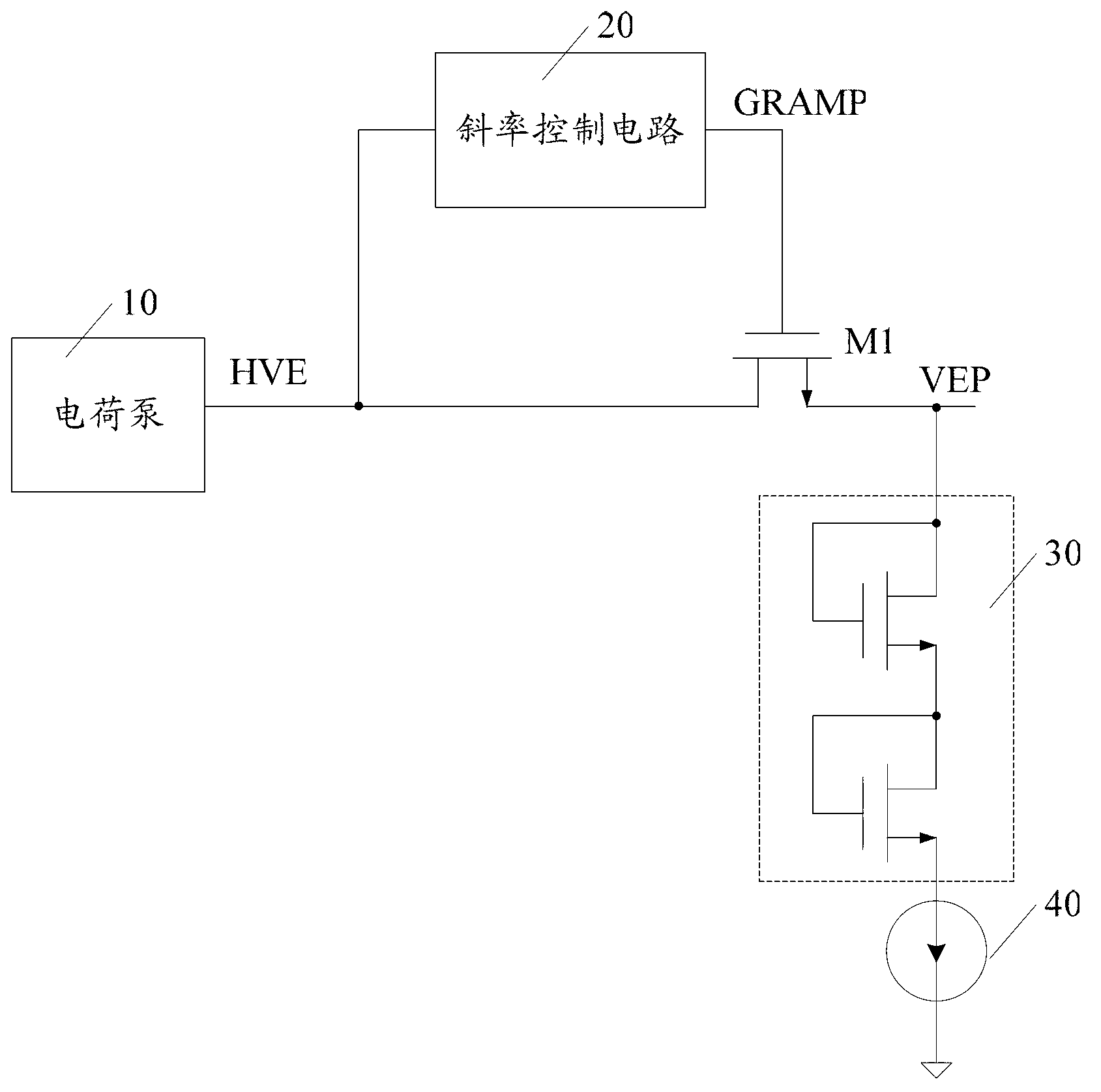
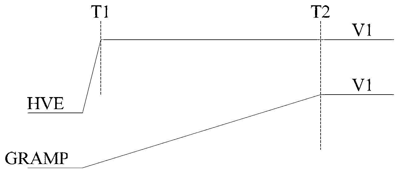
[0029] As mentioned in the background art, figure 1 The output voltage of the regulation circuit shown is not stable. The inventor of the present invention finds through careful study: figure 1 The output voltage VEP of the regulating circuit varies with the drain current I of the transistor M1 D change with changes. When the drain current I D When the larger, the output voltage VEP is smaller, and when the drain current I D The smaller the value is, the larger the output voltage VEP is.

[0030] This unstable voltage will directly affect the erasing operation of subsequent memory cells, so the inventor of the technical solution provides a charge pump output voltage regulator circuit that can output a stable voltage.

[0031] In order to make the above objects, features and advantages of the present invention more comprehensible, specific embodiments of the present invention will be described in detail below in conjunction with the accompanying drawings.

[0032] refer t...


PUM


Abstract

The invention discloses a charge pump output voltage regulating circuit and a storage device. The circuit comprises a booster circuit, a slope control circuit and an output transistor, wherein the input end of the booster circuit is connected with the output end of a charge pump, the booster circuit is suitable for boosting the output voltage of the charge pump to a first voltage, and the voltage difference between the first voltage and the output voltage of the charge pump is more than the threshold voltage of the output transistor; the input end of the slope control circuit is connected with the output end of the booster circuit, the output end of the slope control circuit is connected with the grid of the output transistor, the output voltage of the slope control circuit varies along with the input voltage of the slope control circuit to the first voltage, and the voltage change rate of the output voltage of the slope control circuit is less than the voltage change rate of the input voltage of the slope control circuit; and the drain electrode and the source electrode of the output transistor are respectively connected with the output end of the charge pump and the output end of the regulating circuit. The output voltage of the regulating circuit is stable, so that the misoperation of a subsequent storage unit in an erasing process is reduced.

Description

technical field [0001] The invention relates to the technical field of integrated circuits, in particular to a circuit and memory for adjusting the output voltage of a charge pump. Background technique [0002] At present, semiconductor memories are widely used in various occasions, and semiconductor memories can be classified into volatile memories and nonvolatile memories. Non-volatile memory is more popular due to its ability to retain data in the absence of power. When performing an erasing operation on a non-volatile memory, it is usually necessary to apply a certain erasing voltage to the control gate of the memory unit. [0003] Because of its simple circuit and high efficiency, the charge pump is widely used in semiconductor integrated circuits to provide erasing voltage for semiconductor memory devices for erasing operations of the memory devices. [0004] In the prior art, in order to ensure the accuracy of the erasing operation, it is usually necessary to effect...

Claims


Application Information

Patent Timeline
Patent Type & Authority Applications(China)
IPC IPC(8): H02M3/156H02M3/07G11C16/30
Inventor 杨光军
Owner SHANGHAI HUAHONG GRACE SEMICON MFG CORP
Why Eureka
Try Eureka