
Readout amplifier with process and current compensation

A sense amplifier and current compensation technology, applied in the direction of instruments, static memory, digital memory information, etc., can solve the problems of increasing node IO voltage difference, node IO voltage difference, and decreasing the memory access speed of sense amplifier performance. Improve performance and reduce the effect of voltage variance

Active Publication Date: 2010-07-14
SHANGHAI HUAHONG GRACE SEMICON MFG CORP
View PDF4 Cites 19 Cited by
  • Summary
  • Abstract
  • Description
  • Claims
  • Application Information

AI Technical Summary

Problems solved by technology

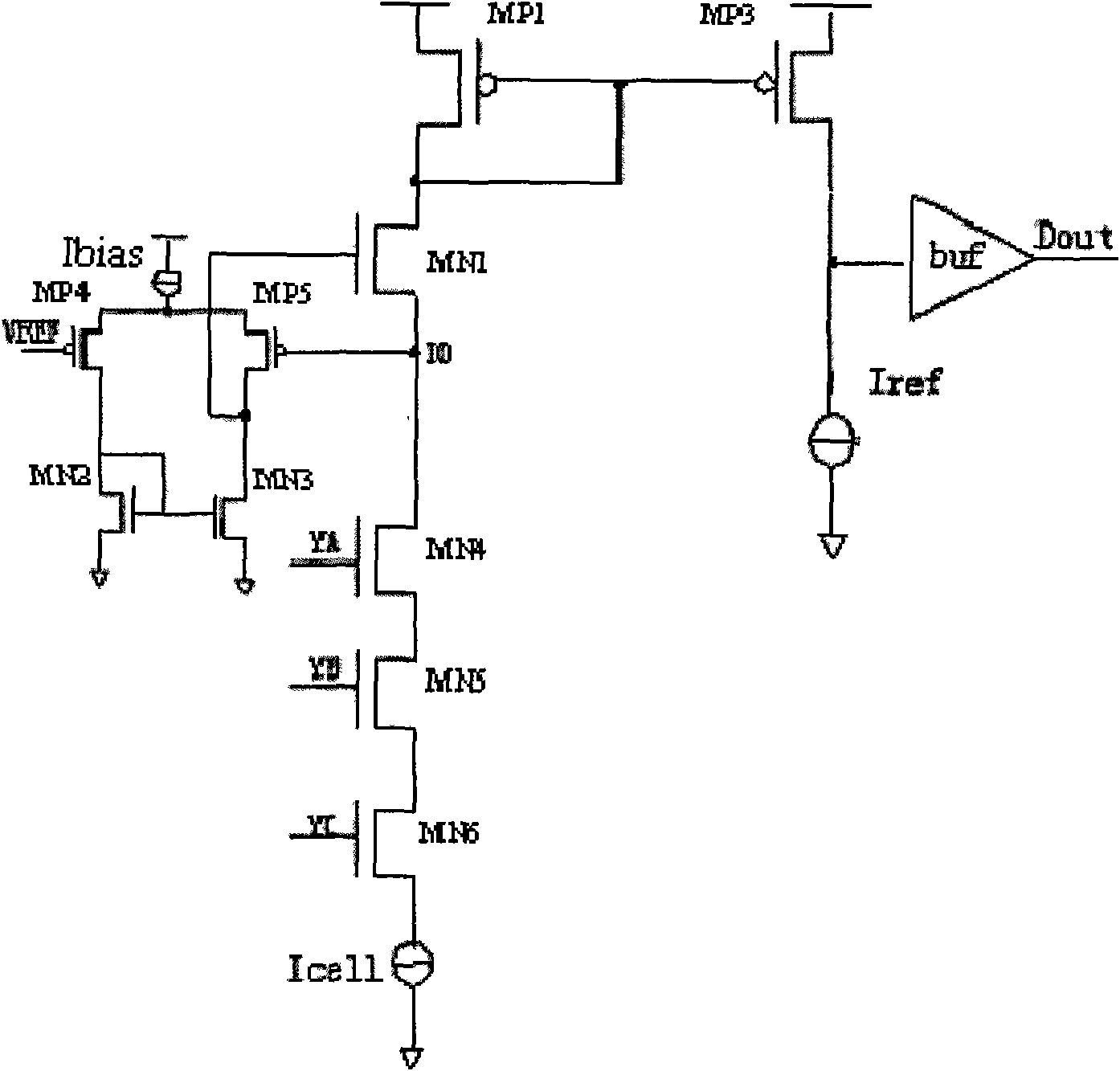
However, due to process reasons, the gate-source voltage V of the NMOS transistor MN1 GS There is a certain difference, which leads to a certain difference in the voltage of the node IO. In addition, because the storage content of the memory corresponds to a different size of the storage cell current Icell, the voltage difference of the node IO is further increased, both of which will lead to the performance of the sense amplifier. and a decrease in memory access speed
[0009] In summary, it can be seen that the current sense amplifiers of the prior art may have differences in the voltage of the node IO (bit line) due to process reasons and the size of the memory cell current Icell corresponding to different memory storage contents, resulting in the performance of the sense amplifier. and memory access speed drop, so it is necessary to propose improved technical means to solve this problem

Method used


Image

  • Readout amplifier with process and current compensation
  • Readout amplifier with process and current compensation
  • Readout amplifier with process and current compensation

Examples


Embodiment Construction

[0033] The implementation of the present invention is described below through specific examples and in conjunction with the accompanying drawings, and those skilled in the art can easily understand other advantages and effects of the present invention from the content disclosed in this specification. The present invention can also be implemented or applied through other different specific examples, and various modifications and changes can be made to the details in this specification based on different viewpoints and applications without departing from the spirit of the present invention.

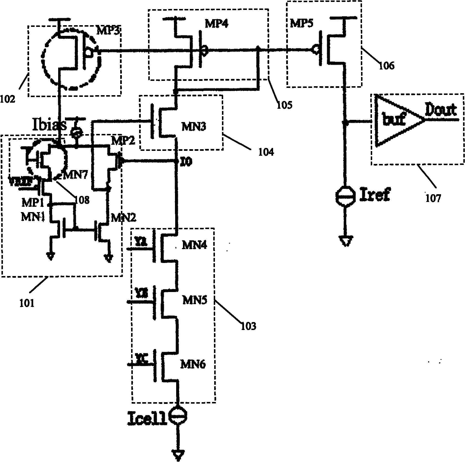
[0034] figure 2 It is a circuit structure diagram of a sense amplifier with process and current compensation in the present invention. like figure 2 As shown, a sense amplifier with process and current compensation of the present invention includes a differential amplifier circuit 101, a mirror circuit 102, a control logic circuit 103, a clamp circuit 104, a memory cell current transfer ...


PUM


Abstract

The invention discloses a readout amplifier with process and current compensation. By additionally arranging an imag mirroring circuit for mirroringimaging current signals formed by an access memory cell at the source electrode of a second differential amplifying tube and the grid electrode of a current transferring circuit of a memory cell, and additionally arranging a seventh NMOS (N-channel metal oxide semiconductor) tube between the source electrode of a first differential amplifying tube and the source electrode of the second differential amplifying tube, when the current signals of the memory cell are larger, the grid source voltage of a third NMOS tube is increased, and when the current signals of the memory cell are smaller, the grid source voltage of the third NMOS tube is reduced, thereby achieving the purpose of reducing the voltage difference of bit lines and improving the performance of the readout amplifier and the access speed of the memory.

Description

technical field [0001] The present invention relates to a sense amplifier for semiconductor memory circuits, and more particularly to a sense amplifier for semiconductor memory circuits with process and current compensation. Background technique [0002] Semiconductor memories are generally considered to be very important components in digital integrated circuits, and they play a vital role in building microprocessor-based application systems. In recent years, more and more people have embedded various memories in the processor to make the processor have higher integration and faster working speed, so the performance of the memory array and its peripheral circuits is largely determined. It determines the working condition of the whole system, including speed, power consumption and so on. [0003] The most important among various peripheral devices of the semiconductor memory is the sense amplifier. Since the sense amplifier is usually used to sample the slight signal chang...

Claims


Application Information

Patent Timeline
Patent Type & Authority Applications(China)
IPC IPC(8): G11C7/06
Inventor 杨光军
Owner SHANGHAI HUAHONG GRACE SEMICON MFG CORP
Learn More