Liquid crystal display device

a liquid crystal display and display device technology, applied in the field of liquid crystal display devices, can solve the problems of ineffective reduction of the thickness of the liquid crystal panel, limited display area inability to reduce the thickness so as to facilitate the minimization of the liquid crystal display device, reduce the area of the fpc film, and achieve the effect of compact crystal liquid display devi

Inactive Publication Date: 2006-03-14
HANNSTAR DISPLAY CORPORATION
View PDF7 Cites 19 Cited by
  • Summary
  • Abstract
  • Description
  • Claims
  • Application Information

AI Technical Summary

Benefits of technology

[0011]The liquid crystal display device of the present invention provides the following advantages. Since the power circuit and the gamma compensating circuit are designed on the FPC film, voltage levels and gamma levels supplied to the driver IC chips will not generate voltage drops due to the wiring limitation of the glass substrate. Since the power circuit and the gamma compensating circuit are not required to be wired on the glass substrate, the peripheral area of the glass substrate can be reduced to facilitate the minimization of the liquid crystal display device. Since the driver IC chips are mounted on the glass substrate for facilitating the reduction of the FPC film in area, the dimension of the FPC film in width can be substantially equal to the dimension of the crystal liquid panel in thickness such that the FPC film can be folded to the side portion of the crystal liquid panel rather than the back portion so as to achieve the object of the compactness of the crystal liquid display device.

Problems solved by technology

However, the liquid crystal display device with the above-described tape carrier packages and common printed wiring boards has the following drawbacks.
Secondly, the minimization of the liquid crystal display device or dimension of the display area of the liquid crystal panel is limited by an occupied space of the tape carrier packages and the common printed wiring board.
Lastly, in a liquid crystal module assembling process, the common printed wiring boards are bent to the back of the liquid crystal panel such that the thickness of the liquid crystal panel is unable to be decreased effectively.

Method used


Image

  • Liquid crystal display device
  • Liquid crystal display device
  • Liquid crystal display device

Examples


Embodiment Construction

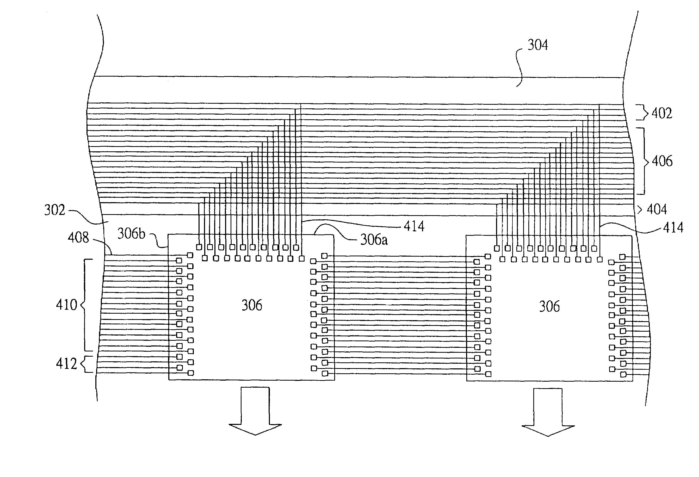
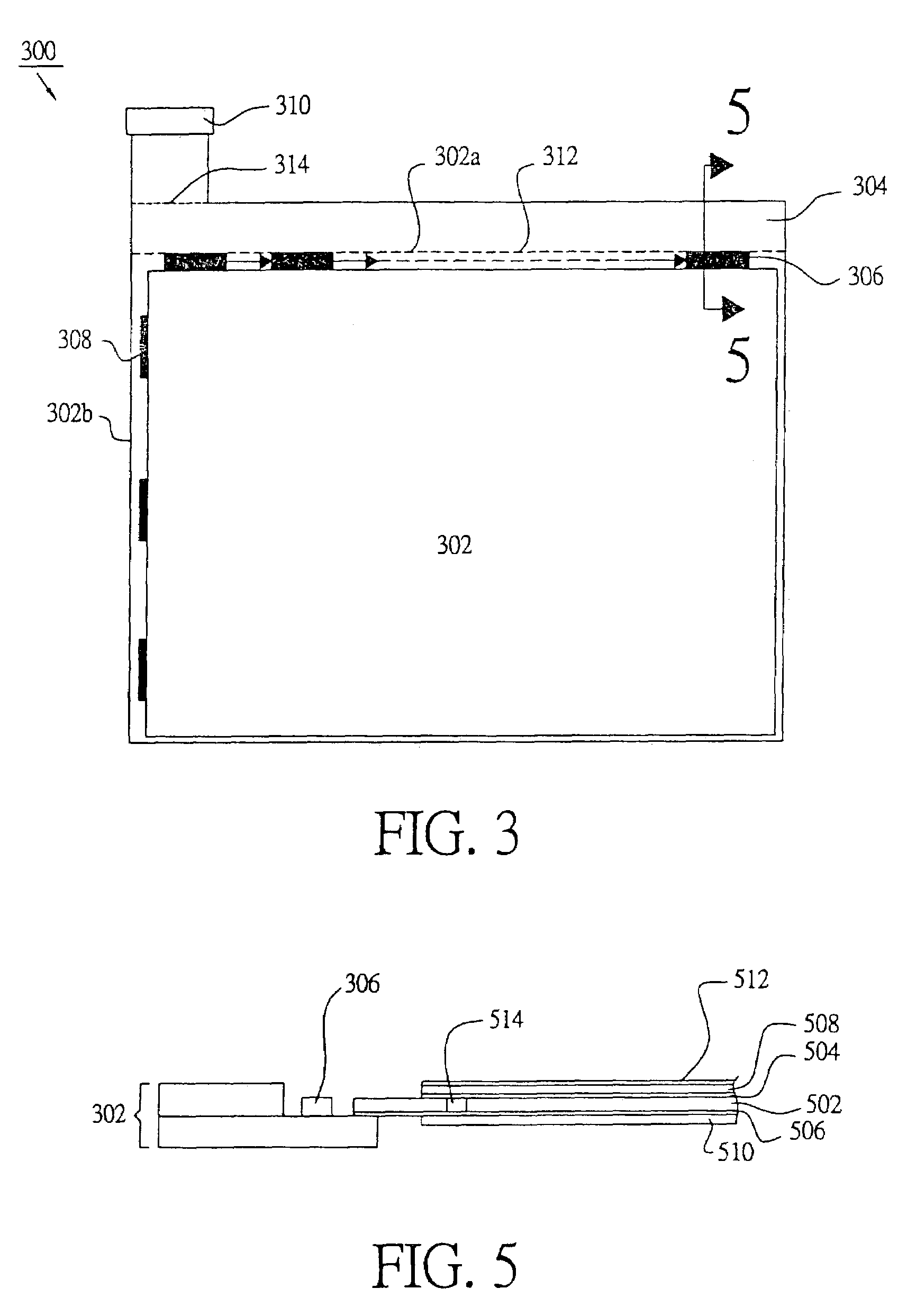
[0020]Referring to FIG. 3, it shows a liquid crystal display device 300 according to an embodiment of the present invention. The liquid crystal display device 300 mainly comprises a liquid crystal panel 302, a FPC film 304 connected to the liquid crystal panel 302, and a plurality of driver IC chips 306, 308 mounted on the liquid crystal panel 302, and an external controller 310 connected to the FPC film 304 for driving the driver IC chips 306, 308.

[0021]Those skills in the art should be understood that the liquid crystal panel 302 comprises a liquid crystal layer interposed between an array substrate and an opposite substrate. Both the array substrate and the opposite substrate of the liquid crystal panel 302 have a transparent glass plate used as a base material. The array substrate includes a matrix array of pixel electrodes, scanning lines respectively along the rows of these pixel electrodes, signal lines respectively formed along the columns of these pixel electrodes, and Thin...


PUM

PropertyMeasurementUnit
thicknessaaaaaaaaaa
lengthaaaaaaaaaa
widthaaaaaaaaaa

Abstract

A liquid crystal display device comprises a liquid crystal panel, a flexible printed circuit (FPC) film connecting to the liquid crystal panel, and a plurality of driver IC chips formed on the liquid crystal panel directly. The present invention is characterized in that a power circuit, a gamma compensating circuit and a ground circuit are formed on the FPC film and are electrically connected to each of the driver IC chips respectively and that the driver IC chips are formed on the glass substrate of the liquid crystal panel directly to save the space of the PCB and lower the cost.

Description

RELATED APPLICATIONS[0001]This application is a continuation-in-part of U.S. Ser. No. 10 / 286,762, entitled Liquid Crystal Display Device, filed on Nov. 4, 2002 abandoned.BACKGROUND OF THE INVENTION[0002]1. Field of the Invention[0003]The invention relates to a liquid crystal display device in which drive integrated circuit (IC) chips are mounted on a glass substrate of a liquid crystal panel.[0004]2. Description of the Related Art[0005]As shown in FIG. 1, it shows a conventional liquid crystal display device 10 which mainly comprises a liquid crystal panel 100, a plurality of tape carrier packages (TCPs) 102, and common printed wiring boards 104. The liquid crystal panel 100 has a matrix array of pixel electrodes, a plurality of scanning lines formed along rows of the pixel electrodes, and a plurality of signal lines formed along columns of the pixel electrodes. The common printed wiring board 104 has a driving circuit for transmitting control signals and driving the driver IC chips...

Claims


Application Information

Patent Timeline
Patent Type & Authority Patents(United States)
IPC IPC(8): G02F1/1345G02F1/13G02F1/1362H05K3/36
CPCG02F1/13452H05K3/361
Inventor PAI, FENG TING
Owner HANNSTAR DISPLAY CORPORATION
Why Eureka
Try Eureka