
Image processing device with a processing unit that processes image data in units of one scan line
a processing unit and image data technology, applied in the field of image processing devices, can solve the problems of insufficient processing and low speed of processors, and achieve the effect of reducing the number of pixels of input image data
- Summary
- Abstract
- Description
- Claims
- Application Information
AI Technical Summary
Benefits of technology
Problems solved by technology
Method used
Image

Examples
first embodiment
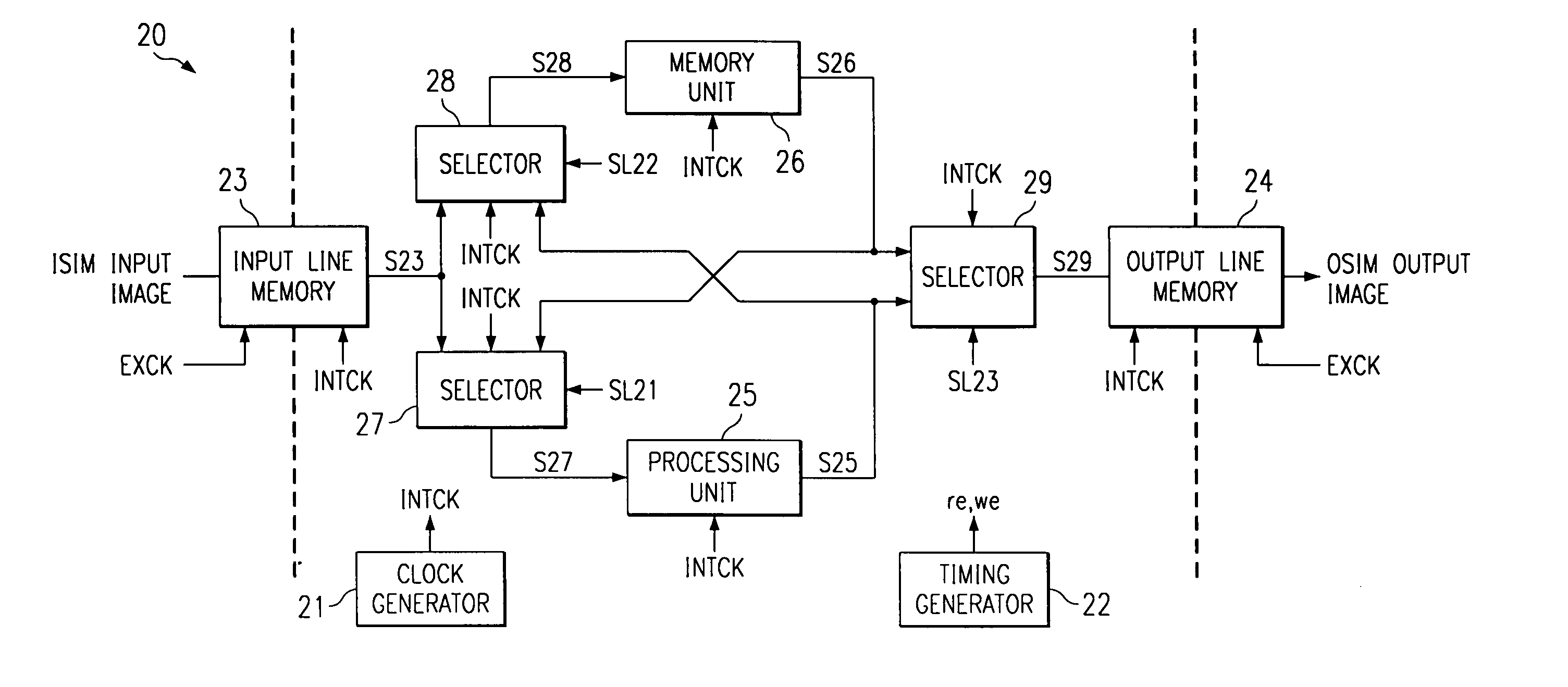
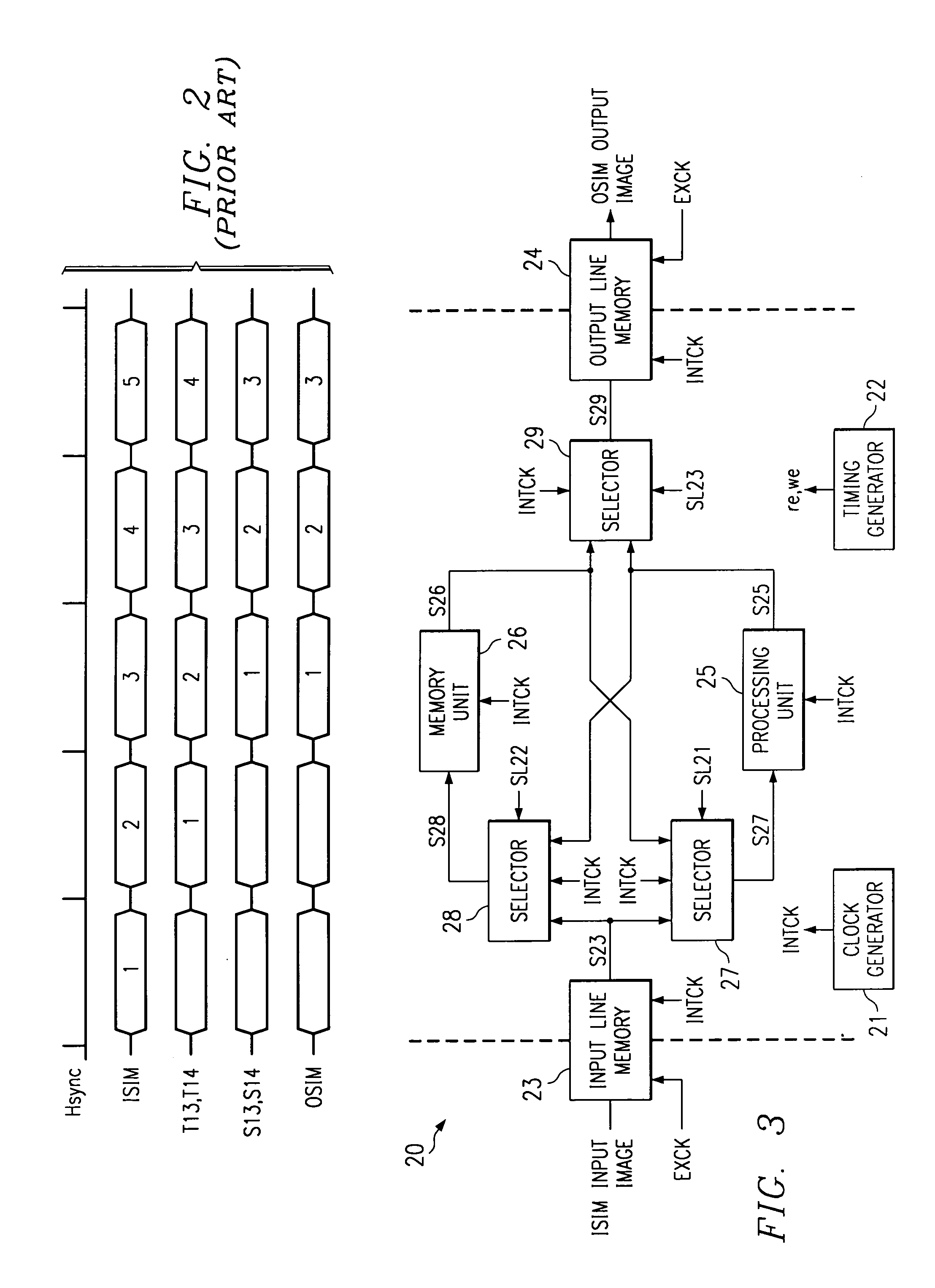
[0060]FIG. 3 is a block diagram illustrating the first embodiment of the image processing device disclosed in the present invention. FIG. 4 is the timing diagram of the image processing device shown in FIG. 3.
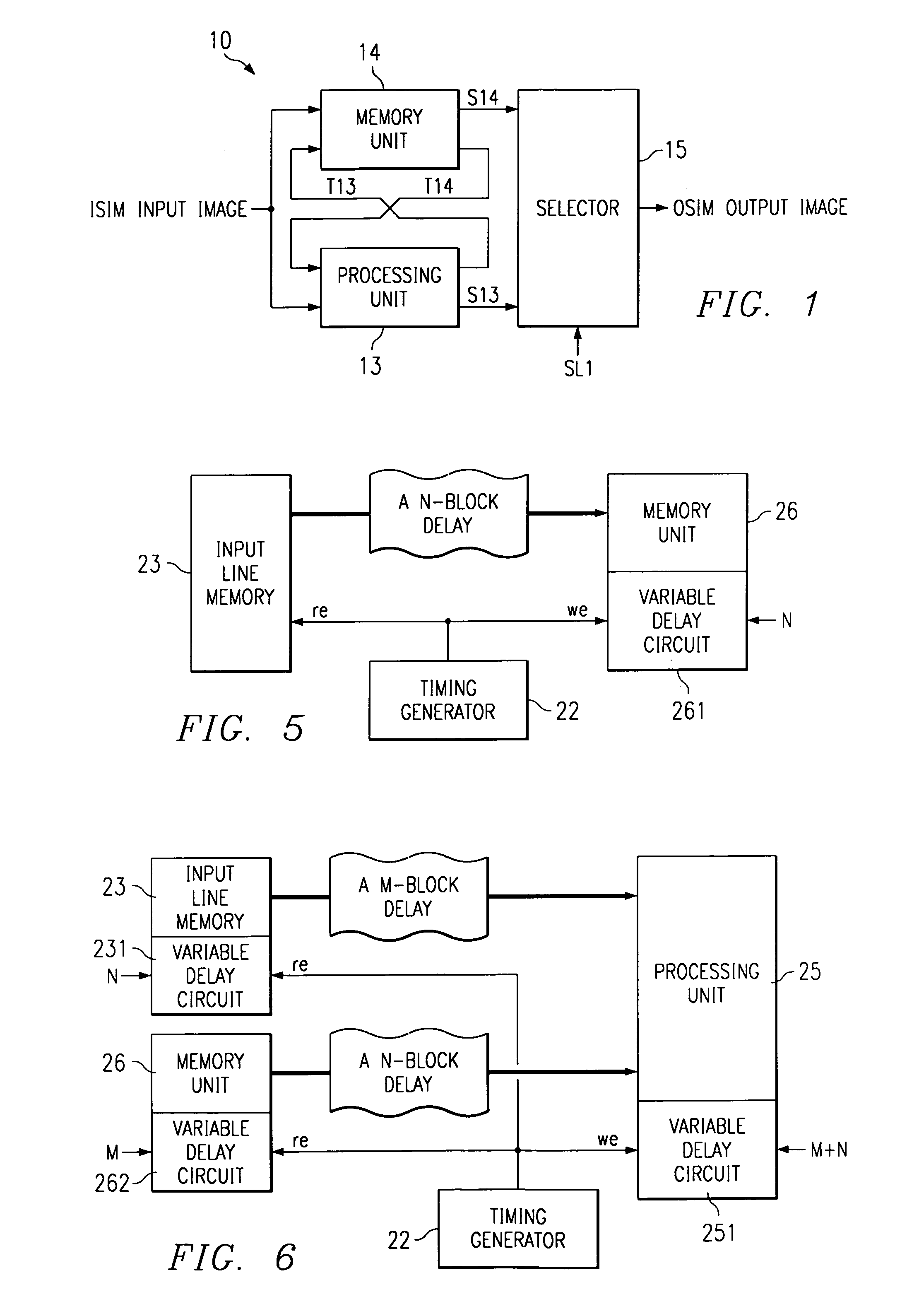
[0061]As shown in FIG. 3, the image processing device 20 disclosed in the first embodiment comprises clock generator 21, timing generator 22, input line memory 23, output line memory 24, processing unit 25, memory unit 26, as well as selectors 27, 28, and 29.
[0062]The transfer part comprises selector 27 (first selector) and selector 28 (second selector).
[0063]Clock generator 21 generates an internal clock signal INTCK of several hundred MHz which is n times faster than the external clock (for example, tens of MHz) and supplies this clock signal to the reading system of input line memory 23, the writing system of output line memory 24, the input / output system of processing unit 25, the writing and reading systems of memory unit 26, and various selectors 27–29.
[0064]Timing genera...
second embodiment
[0099]FIG. 7 is a block diagram illustrating the second embodiment of the image processing device disclosed in the present invention.
[0100]The difference between the second embodiment and said first embodiment is that the transfer speed between the input / output line memory and the memory unit, the operating speed of the processing unit, and the storage speed of the memory unit are different from each other.
[0101]More specifically, for the image processing device 20A disclosed in the second embodiment, processing unit 25A comprises input buffer 252, output buffer 253, and processing circuit 254. Memory unit 26A comprises input buffer 263, output buffer 264, and memory circuit 265. Said input buffers 252 and 263 as well as output buffers 253 and 264 input / output image data operate synchronously with internal clock signal INTCK generated by clock generator 21 (not shown in FIG. 7). Said processing circuit 254 and memory circuit 265 perform calculation and storage synchronously with int...
third embodiment
[0105]FIG. 8 is a block diagram illustrating the third embodiment of the image processing device disclosed in the present invention.
[0106]The difference between the third and second embodiments is as follows: the memory part has multiple input buffers (two in the third embodiment); as a result, a second input line memory is adopted; during the stage when the first input image ISIM1 input from the first input line memory 23-1 to the first input buffer 263-1 of memory unit 26B and the intermediate processing data between processing unit 25B and memory unit 26B, or the second input image ISIM2, which is asynchronous with the scan line of the data output from processing unit 25B or memory unit 26B to output line memory 24, are input to the second input buffer 263-2 of memory unit 26B from the second input line memory 23-2 and are output from output buffer 264, the second image is synchronized with the first image.
[0107]Although the entire circuit is not shown in FIG. 8, the rest of the ...
PUM
 Abstract
Description
Claims
Application Information