
Megasonic cleaning apparatus for fabricating semiconductor device

a cleaning apparatus and semiconductor technology, applied in the direction of cleaning process and apparatus, cleaning using liquids, chemistry apparatus and processes, etc., can solve the problems of poor pattern, semiconductor device inoperativeness, difficult to remove small contamination particles through conventional cleaning methods,

Inactive Publication Date: 2006-03-28
SAMSUNG ELECTRONICS CO LTD
View PDF27 Cites 2 Cited by
  • Summary
  • Abstract
  • Description
  • Claims
  • Application Information

AI Technical Summary

Benefits of technology

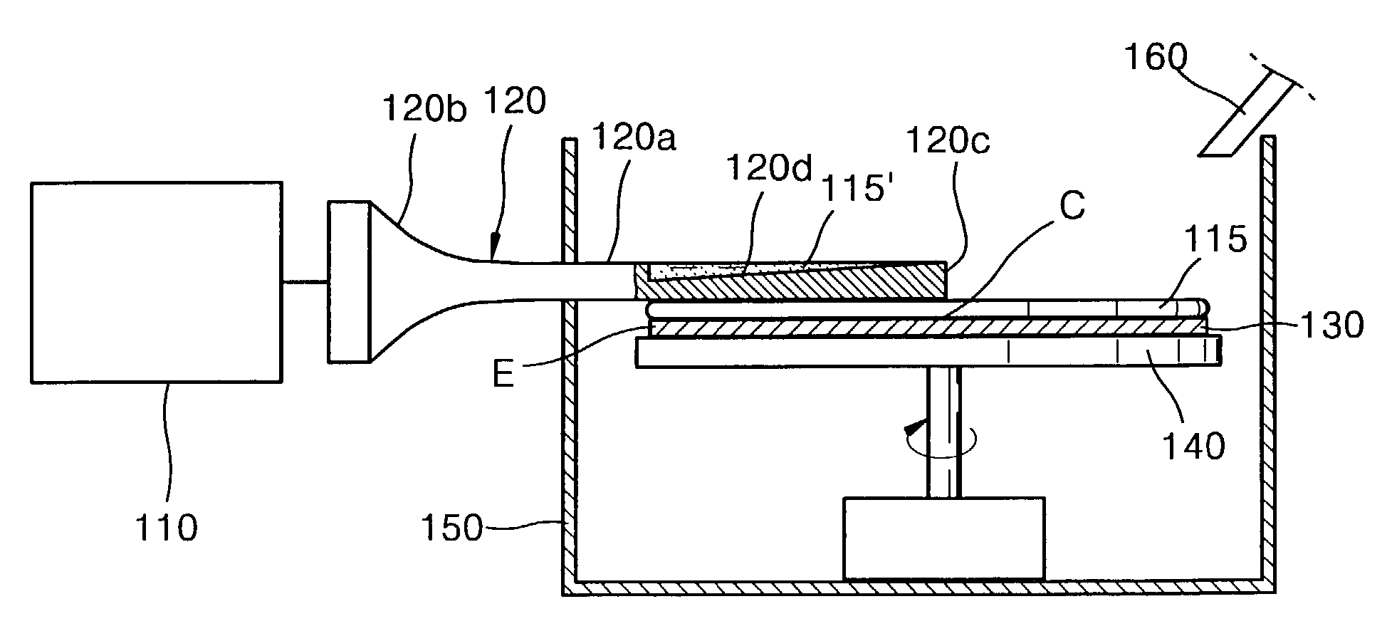
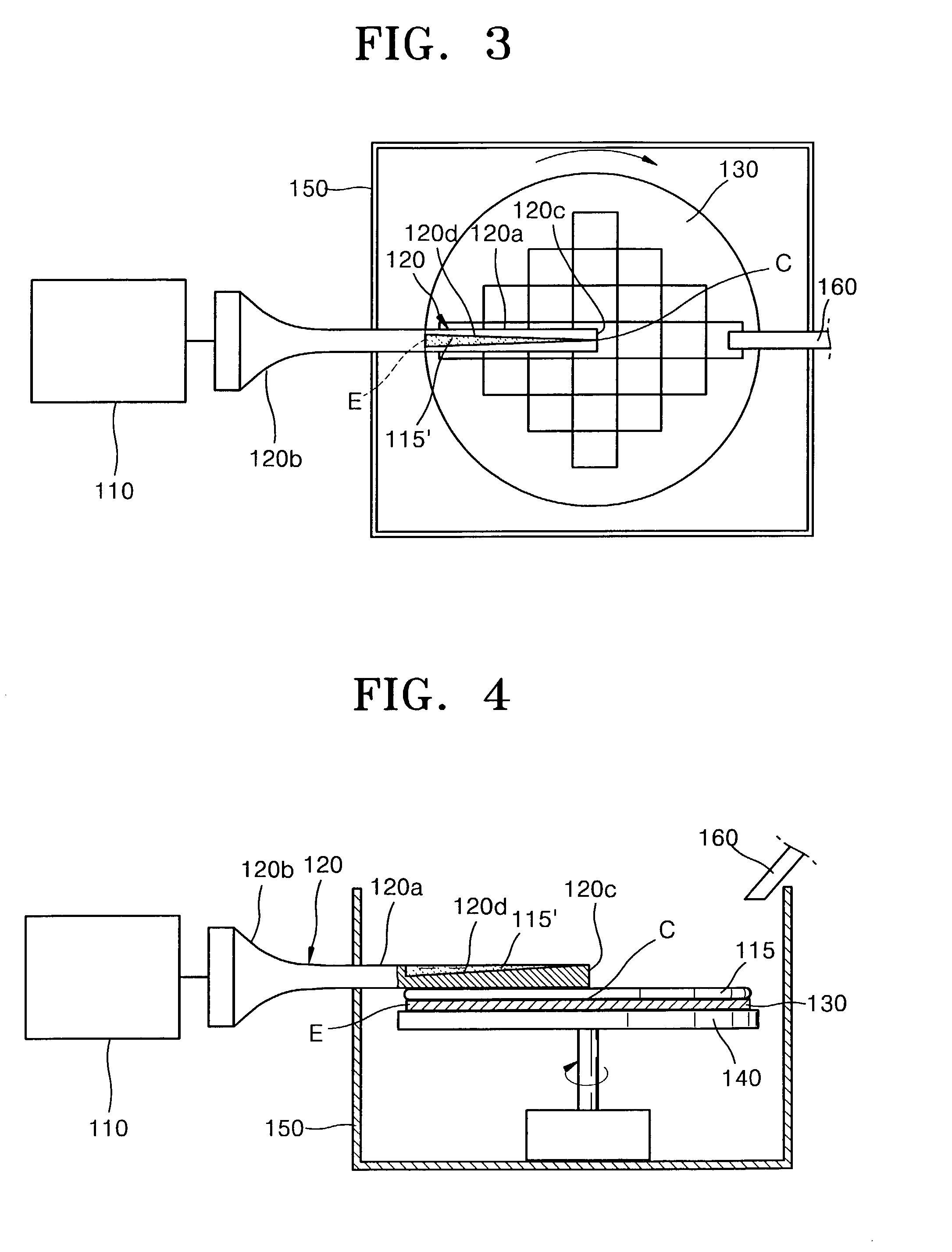
[0015]According to an embodiment of the present invention, the energy transfer rod having a first end and a second end and the diameter of the first end is smaller than that of the second end. The energy transfer rod includes a leading end, an elongated front portion, and a rear portion tapered to have a larger cross-section diameter than the front portion. The leading end is located over the centre of the wafer. The energy transfer rod includes a groove formed on the elongated front portion to make energy distribution uniform over the wafer. The groove is formed from the position of the elongated front portion over the wafer edge to the leading end. The groove is tapered in a semiconical shape to have a maximum radius at the position of the elongated front portion. An end of the groove opposite to the leading end is gradually shallow from a position over the wafer edge. The end of the groove opposite to the leading end is slanted. The groove is filled with the cleaning solution such that a part of energy is dissipated by the cleaning solution filled in the groove.

Problems solved by technology

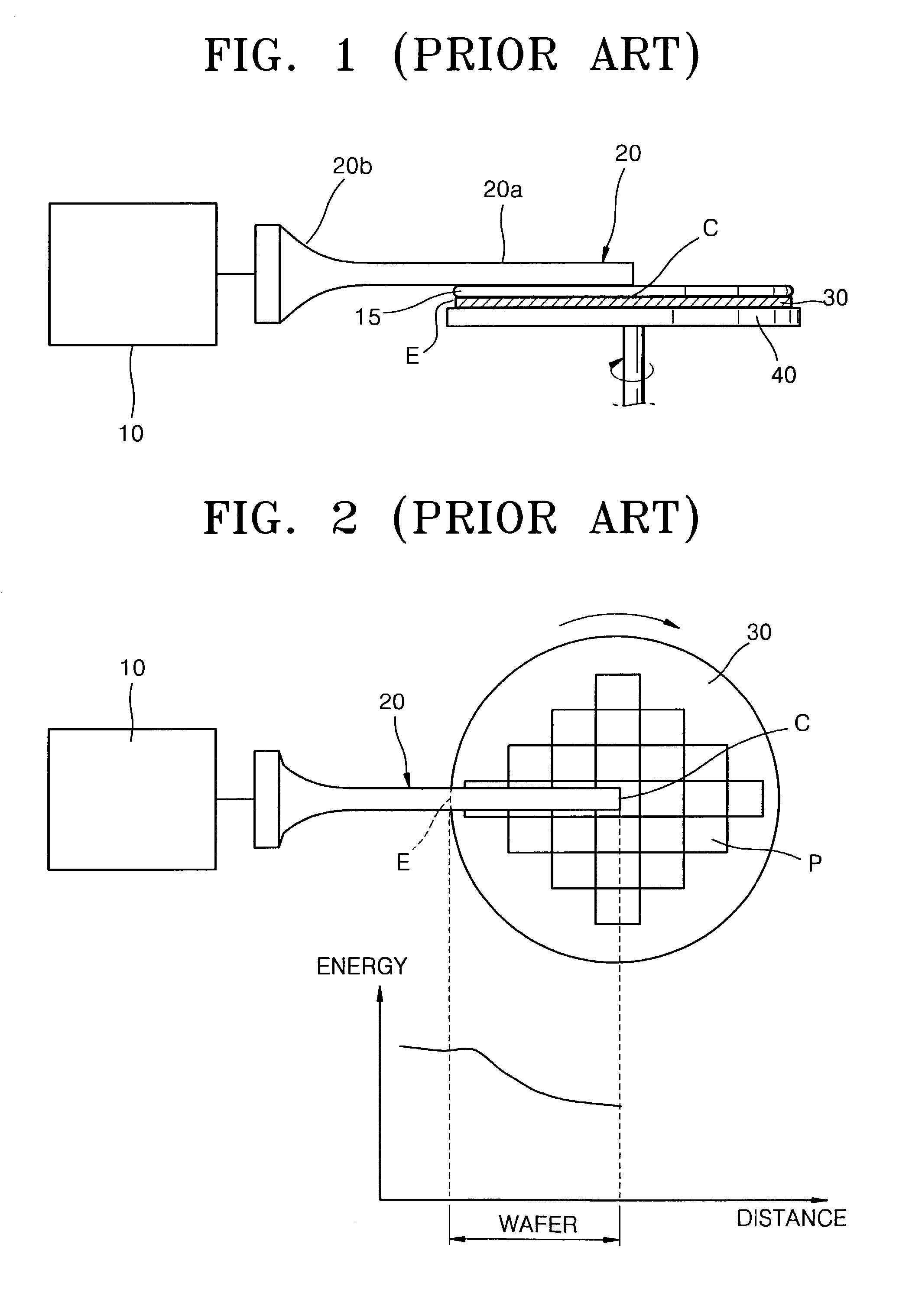
Accordingly, wafer cleaning becomes important because contamination particles existing on the surface of a wafer could cause poor patterns in subsequent processes, for example, contamination particles which remain between the patterns formed of a conductive film could render the semiconductor device inoperative.
Thus, it can be difficult to remove those small contamination particles through conventional cleaning methods because of the strong adhesion force upon a wafer.
However, if the energy amount increases for obtaining a sufficient cleaning effect, the wafer edge E receives excessive energy, leading to a serious problem that patterns P located around the wafer edge E are lifted.

Method used


Image

  • Megasonic cleaning apparatus for fabricating semiconductor device
  • Megasonic cleaning apparatus for fabricating semiconductor device
  • Megasonic cleaning apparatus for fabricating semiconductor device

Examples


Embodiment Construction

[0026]Hereinafter, embodiments of the present invention will be described in detail with reference to the attached drawings. However, the embodiments of the present invention can be modified into various other forms, and the scope of the present invention should not be interpreted as being restricted to the embodiments. The present invention includes alternatives, modifications and equivalents that can be included within the spirit and scope of the invention defined by the attached claims. Like reference numerals in the drawings denote the same members.

[0027]FIG. 3 is a top view of a megasonic cleaning apparatus according to an embodiment of the present invention and FIG. 4 is a side cross-sectional view of the apparatus of FIG. 3.

[0028]Referring to FIGS. 3 and 4, the megasonic cleaning apparatus includes a piezoelectric transducer 110 and an energy transfer rod 120 connected to the piezoelectric transducer 110 and disposed over a wafer 130 in a radial direction. The piezoelectric t...


PUM


Abstract

A megasonic cleaning apparatus is provided for removing contamination particles on a wafer. The megasonic cleaning apparatus includes a piezoelectric transducer and an energy transfer rod. The piezoelectric transducer is for generating megasonic energy. The energy transfer rod installed over the wafer along a radial direction of the wafer is for distributing the megasonic energy to cleaning solution over the wafer and for vibrating the cleaning solution. The energy transfer rod is shaped and sized to uniformly distribute energy in the radial direction of the wafer through the cleaning solution to remove the contamination particles from the wafer.

Description

BACKGROUND OF THE INVENTION[0001]1. Field of the Invention[0002]The present invention relates to a megasonic cleaning apparatus for fabricating a semiconductor device, and more particularly, to a megasonic cleaning apparatus capable of obtaining a sufficient level of cleaning effect and preventing pattern lifting.[0003]2. Description of the Related Art[0004]With increases in the integration of semiconductor devices, the size of patterns and the interval between patterns become very small. Accordingly, wafer cleaning becomes important because contamination particles existing on the surface of a wafer could cause poor patterns in subsequent processes, for example, contamination particles which remain between the patterns formed of a conductive film could render the semiconductor device inoperative.[0005]With a reduction of the size of a fine pattern to 1 μm or less, the permissible size of a contamination particle also decreases. Thus, it can be difficult to remove those small contami...

Claims


Application Information

Patent Timeline
Patent Type & Authority Patents(United States)
IPC IPC(8): B08B3/12B08B3/00H01L21/304H01L21/00
CPCB08B3/12H01L21/67051Y10S134/902H01L21/304
Inventor YOON, BYOUNG-MOONYEO, IN-JUNHAH, SANG-ROKKIM, KYUNG-HYUNJO, HYUN-HONAM, JEONG-LIM
Owner SAMSUNG ELECTRONICS CO LTD
Learn More