Solid-state image sensor with the optical center of microlenses shifted from the center of photo-sensors for increasing the convergence ratio

a technology microlenses, which is applied in the field of solid-state image sensor, can solve the problems of poor incident light quantity, poor luminance of produced signals, and the inability of primary photosensitive cells to identify the level of incident light exceeding a certain intensity level, so as to prevent image quality from being degraded and reduce the sensitivity of low-sensitivity cells

Active Publication Date: 2006-03-28
SAMSUNG ELECTRONICS CO LTD
View PDF5 Cites 9 Cited by
  • Summary
  • Abstract
  • Description
  • Claims
  • Application Information

AI Technical Summary

Benefits of technology

[0014]It is an object of the present invention to provide a solid-state image sensor in which a lowering of the sensitivity of low-sensitivity cells is minimi

Problems solved by technology

Because the optical aperture area, or opening region, of the primary photosensitive cells is broader, its sensitivity is heightened, and, however, the primary photosensitive cell cannot identify the level of the incident light exceeding a certain intensity level.
More specifically, in the vicinity of the edge of a photosensitive array of the image sensor, the light incident to the photo-sensors is often inclined and the direction of the inclination is one-sided specifically to the edge, so that the quantity of the incident light is poorer than one incident to the photo-sens

Method used


Image

  • Solid-state image sensor with the optical center of microlenses shifted from the center of photo-sensors for increasing the convergence ratio
  • Solid-state image sensor with the optical center of microlenses shifted from the center of photo-sensors for increasing the convergence ratio
  • Solid-state image sensor with the optical center of microlenses shifted from the center of photo-sensors for increasing the convergence ratio

Examples


Embodiment Construction

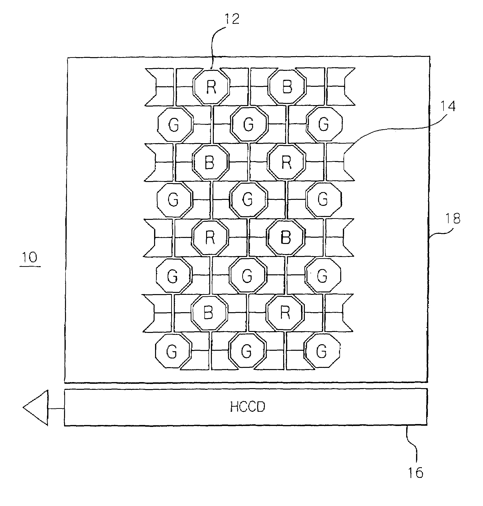
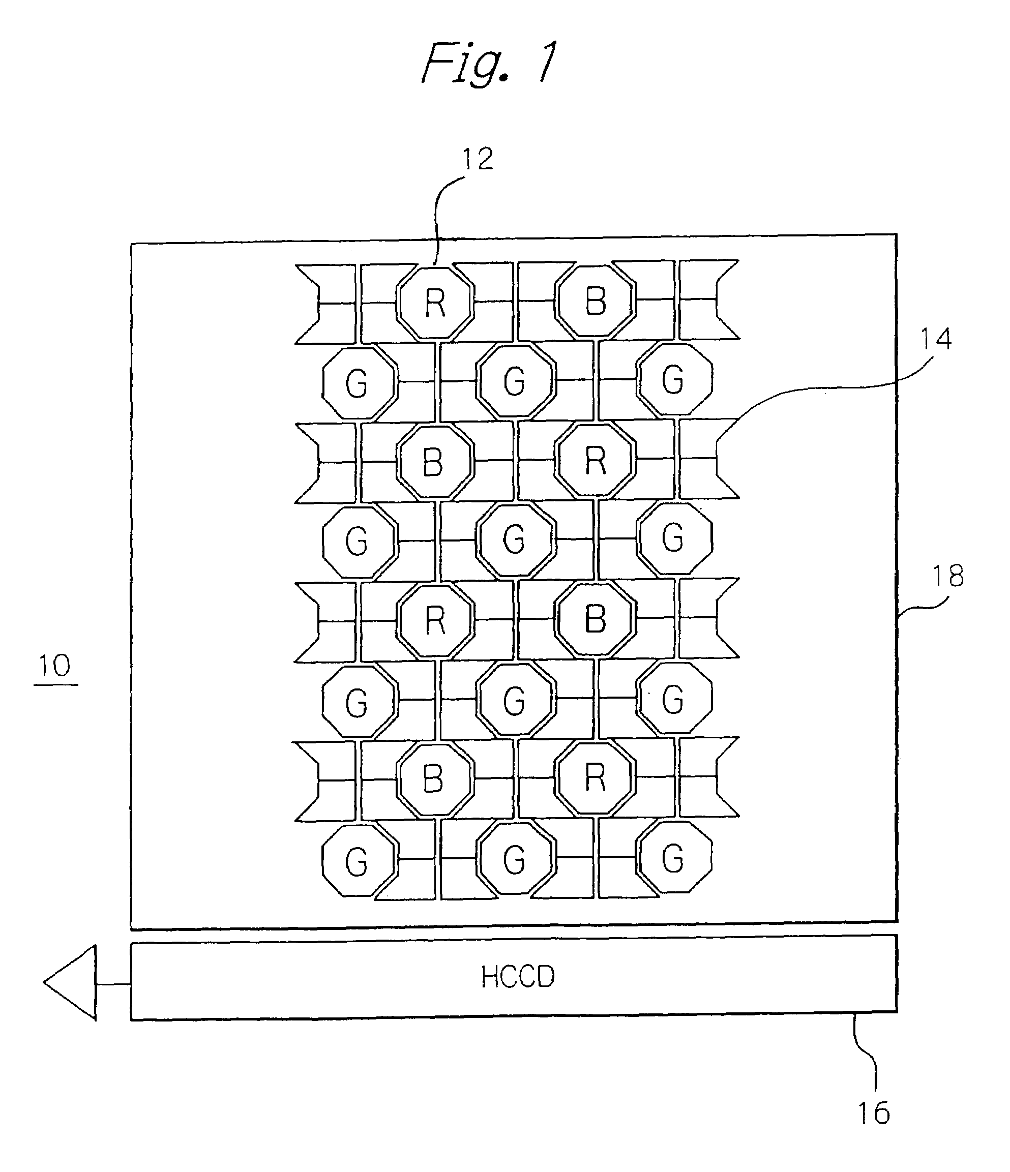
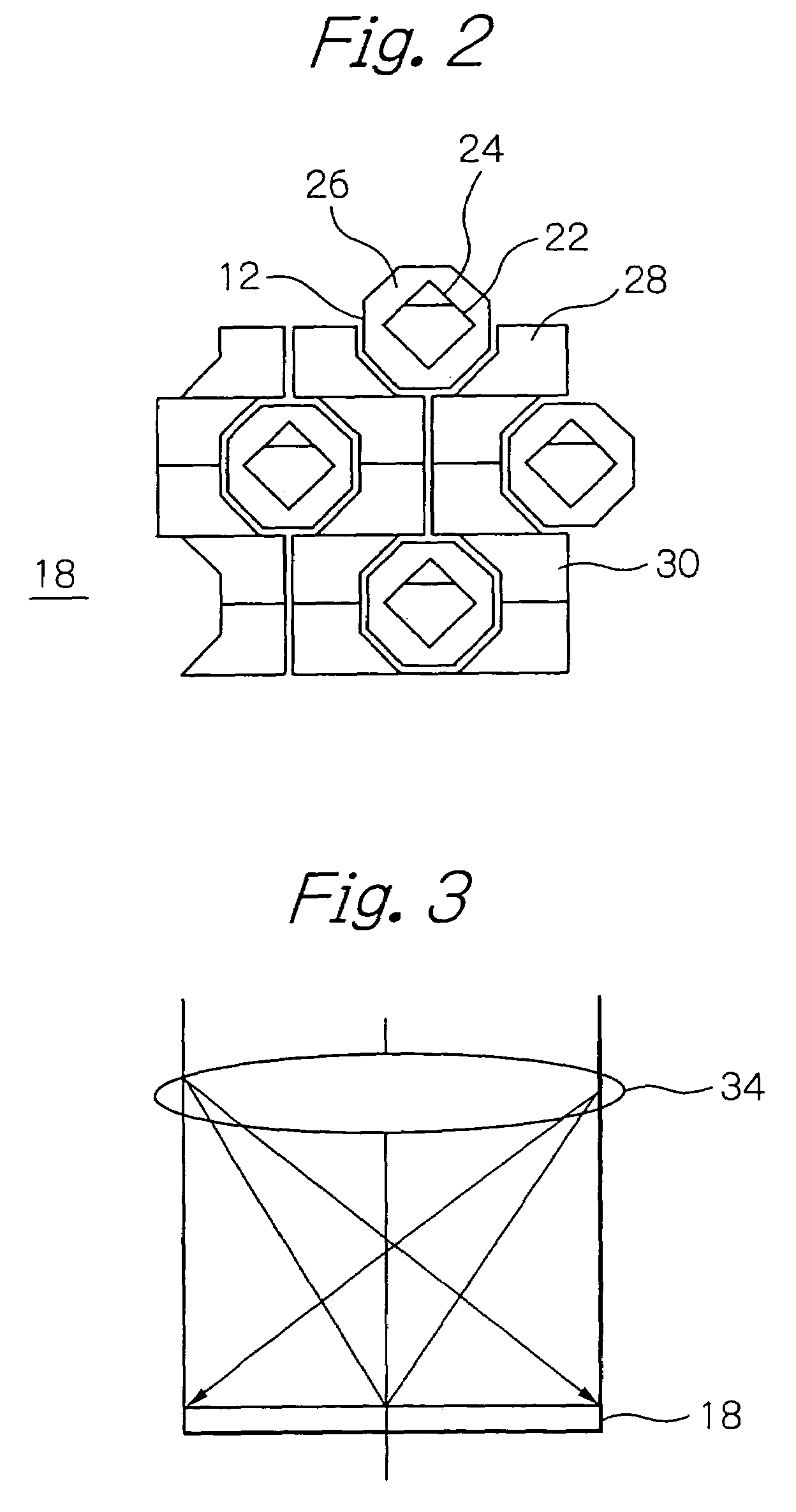
[0030]Preferred embodiments of the solid-state image sensor in accordance with the present invention will be described hereinafter. Briefly, in the illustrative embodiments described, each of the photo-sensors forming a photosensitive array includes a set of, e.g. a pair of, photosensitive cells and a microlens. The photoelectric sensitivity, or transduction efficiency, of the photosensitive cells differs from each other in terms of the size of the opening regions, or optical aperture areas. This successfully broadens the dynamic range.

[0031]Further, the microlenses of the photo-sensors causing light to respectively converge to the opening regions of the photosensitive cells are conveniently formed so that each of the microlenses has its center shifted from the center of the photo-sensor. Consequently, particularly in vicinity of the edges of the photosensitive array, the convergence or concentration ratio of the photosensitive cells, especially low-sensitivity cells, is increased, ...


PUM


Abstract

A solid-state image sensor includes a photosensitive array capturing an optical image representative of a desired scene. The photosensitive array includes photo-sensors arranged in a direction of row and a direction of column, and microlenses each causing incident light to converge to the corresponding photo-sensor. Each photo-sensor corresponds to a particular pixel included in the photosensitive array. Each photo-sensor is made up of a higher- and a lower-sensitivity photosensitive cell for photoelectrically transducing incident light to electric signal charges. Each photo-sensor includes a primary and a secondary photosensitive cell respectively having higher-sensitivity and lower-sensitivity for photoelectrically transducing the incident light. Each microlens has its optical center shifted from the center of the corresponding photo-sensor toward the center of the photosensitive array.

Description

[0001]This Nonprovisional application claims priority under 35 U.S.C. § 119(a) on Patent Application No(s). 2002-323859 filed in JAPAN on Nov. 7, 2002, the entire contents of which are hereby incorporated by reference.BACKGROUND OF THE INVENTION[0002]1. Field of the Invention[0003]The present invention relates to a solid-state image sensor having an array of photo-sensors, each of which has a set of photosensitive cells different in sensitivity from each other and a microlens converging incident light.[0004]2. Description of the Background Art[0005]As known in the art, a solid-state image sensor of the type is available which actualizes a broader dynamic range for using a primary and a secondary photosensitive cell, which are different in optical aperture area, i.e. photo-sensitivity, from each other. Because the optical aperture area, or opening region, of the primary photosensitive cells is broader, its sensitivity is heightened, and, however, the primary photosensitive cell canno...

Claims


Application Information

Patent Timeline
IPC IPC(8): H01J3/14H01J40/14H01J5/16H01L27/14H01L27/00H01L27/146H01L31/0232H04N5/335H04N5/361H04N5/369
CPCH01L27/14603H01L27/14643H01L27/14627H01L27/146
Inventor ODA, KAZUYAKOBAYASHI, HIROKAZU
Owner SAMSUNG ELECTRONICS CO LTD
Why Eureka
Try Eureka