Methods and apparatus for thermally coupling a heat sink to a circuit board component

a technology of circuit board components and heat sinks, which is applied in the direction of cooling/ventilation/heating modifications, semiconductor devices, semiconductor/solid-state device details, etc., can solve the problems of increasing the risk of ics failure, mechanical tolerance differences, and the like, and achieves the effect of minimizing the risk of fracture of the solder joint, and limiting the amount of stress

Inactive Publication Date: 2006-03-28
CISCO TECH INC
View PDF8 Cites 55 Cited by
  • Summary
  • Abstract
  • Description
  • Claims
  • Application Information

AI Technical Summary

Benefits of technology

[0008]To minimize the amount of stress generated by a heat sink on the circuit board components, manufacturers conventionally use custom designed heat sinks. Such custom designed heat sinks apply a controlled amount of stress on the associated circuit board components during operation, where the applied stress is less than the fracture stress of the solder joints of the solder ball array. The custom heat sinks, however, are typically designed on a case-by-case basis and are typically specific to a particular application. Use of such custom heat sinks, therefore, is relatively costly and increases the cost of goods sold (COGS) for a circuit board utilizing custom heat sinks.
[0010]By contrast to the prior heat sink attachment mechanisms, embodiments of the present invention significantly overcome such deficiencies and provide mechanisms and techniques for thermally coupling a heat sink to a circuit board component. A heat sink has a flexure member, attached to a base of the heat sink and located between the base and an associated circuit board component. As the heat sink attaches to a circuit board carrying the circuit board component, the flexure member conforms to the surface of the circuit board component, thereby thermally contacting the circuit board component. The flexure member absorbs local tolerance differences on the circuit board component to provide a relatively uniform stress across the surface of the circuit board component. The flexure member also limits the amount of stress generated by the heat sink on the circuit board component when the heat sink attaches to the circuit board. When used in conjunction with a heat sink spanning several circuit board components, the flexure member absorbs global tolerance differences among the circuit board components, thereby providing relatively uniform stresses to all of the circuit board components and limiting the amount of stress experienced by any one circuit board component.
[0011]In one arrangement, a heat sink assembly has a heat sink having a base and a flexure member configured to position between the base of the heat sink and a circuit board component of a circuit board. The flexure member has an attachment portion fastened to, and in thermal communication with, the heat sink. The flexure member also has a deflection portion integrally formed with the attachment portion where the deflection portion is configured to thermally communicate with the circuit board component and is configured to conform to a surface of the circuit board component during attachment of the heat sink to the circuit board. With the deflection member conforming to the surface of the circuit board component, the heat sink assembly limits the amount of stress generated on the circuit board component, thereby minimizing a risk of fracture of a solder joint between the circuit board component and associated circuit board caused by “overloading” of the circuit board component.
[0012]In one arrangement, the deflection portion defines a substantially curved portion relative to the attachment portion where the substantially curved portion is configured to flatten relative to the circuit board component surface during attachment of the heat sink to the circuit board. The substantially curved portion provides contact between the heat sink and a package die center of the circuit board component where the package die center is defined as the approximate heat source or the approximate location of the circuit board component that generates the largest amount of heat relative to the circuit board component. The substantially the curved portion provides thermal contact between the heat sink and the heat source of the circuit board component and, therefore, relatively efficient thermal dissipation of heat for the circuit board component.
[0013]In one arrangement, the flexure member has multiple attachment portions fastened to, and in thermal communication with, the heat sink. The flexure member also has multiple deflection portions integrally formed with the attachment portions. Each of the plurality of deflection portions are located between two adjacent attachment portions. Each of the plurality of the deflection portions configured to thermally communicate with the circuit board component and configured to conform to the surface of the circuit board component during attachment of the heat sink to the circuit board. Configuring the flexure member with multiple deflection portions allows the flexure member, and the heat sink, to thermally contact multiple circuit board components and, therefore, provide a relatively large thermal transfer (e.g., cooling) capacity to the circuit board assembly.

Problems solved by technology

Conventional techniques for thermally coupling a heat sink to a circuit board component suffer from a variety of deficiencies.
Mechanical tolerance differences exist, however, among IC packages on conventional circuit boards.
The mechanical tolerance differences among the IC packages, however, cause the ganged heat sink to generate potentially large stresses on one or more of the IC packages, thereby increasing the risk of failure of the ICs.
Such stress can fracture the solder joints connecting the solder balls to the corresponding surface mount pads oh the circuit board and lead to the malfunctioning of the ICs.
Use of such custom heat sinks, therefore, is relatively costly and increases the cost of goods sold (COGS) for a circuit board utilizing custom heat sinks.

Method used


Image

  • Methods and apparatus for thermally coupling a heat sink to a circuit board component
  • Methods and apparatus for thermally coupling a heat sink to a circuit board component
  • Methods and apparatus for thermally coupling a heat sink to a circuit board component

Examples


Embodiment Construction

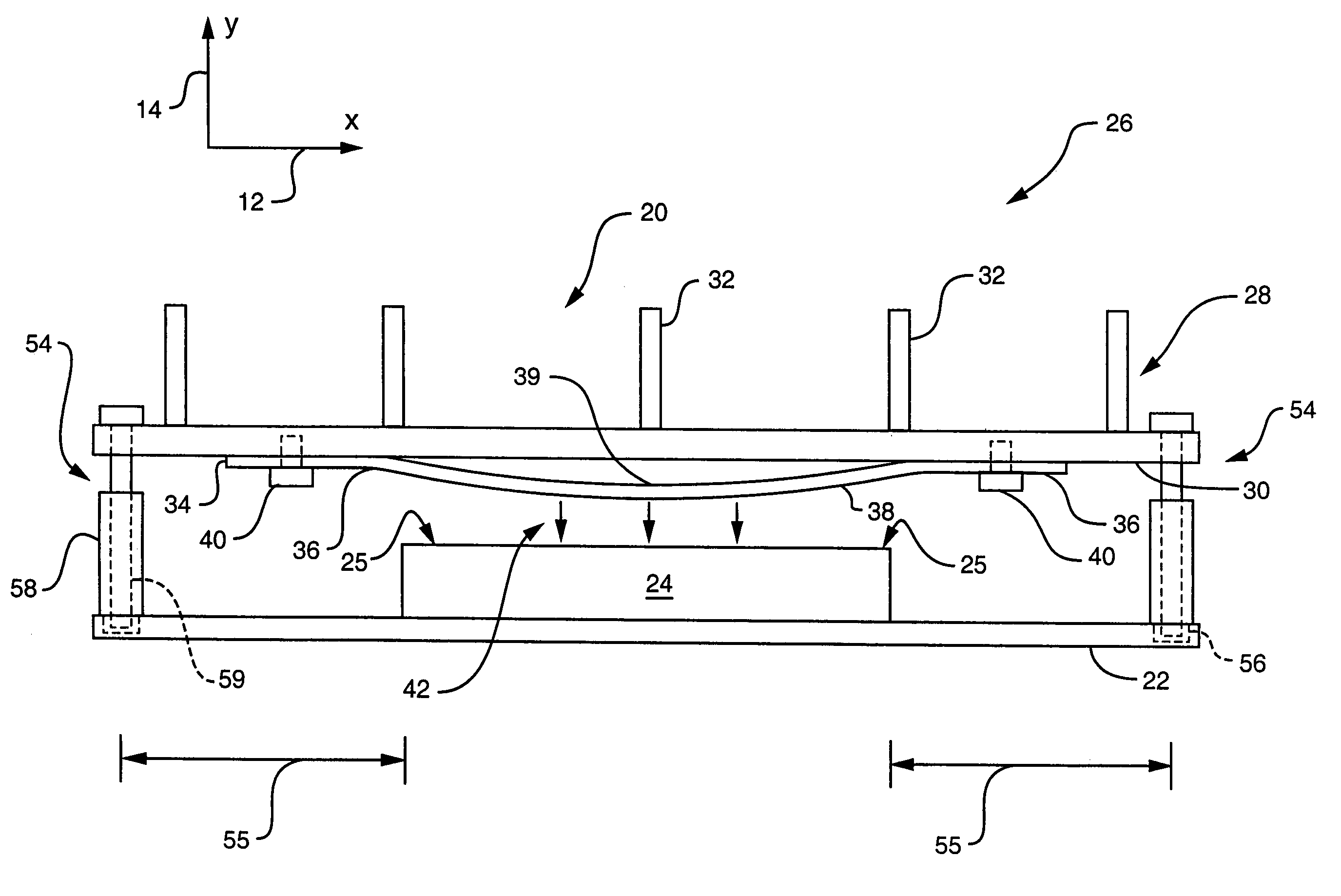
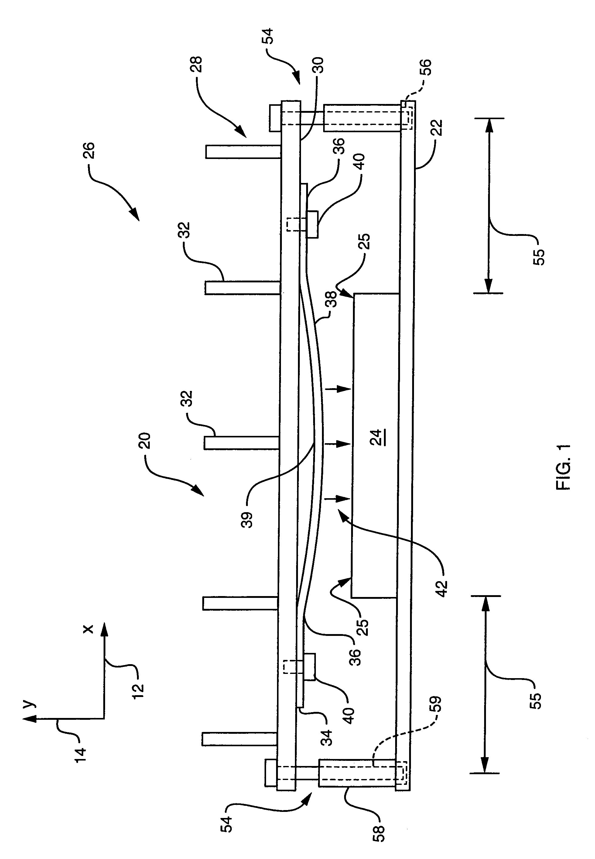
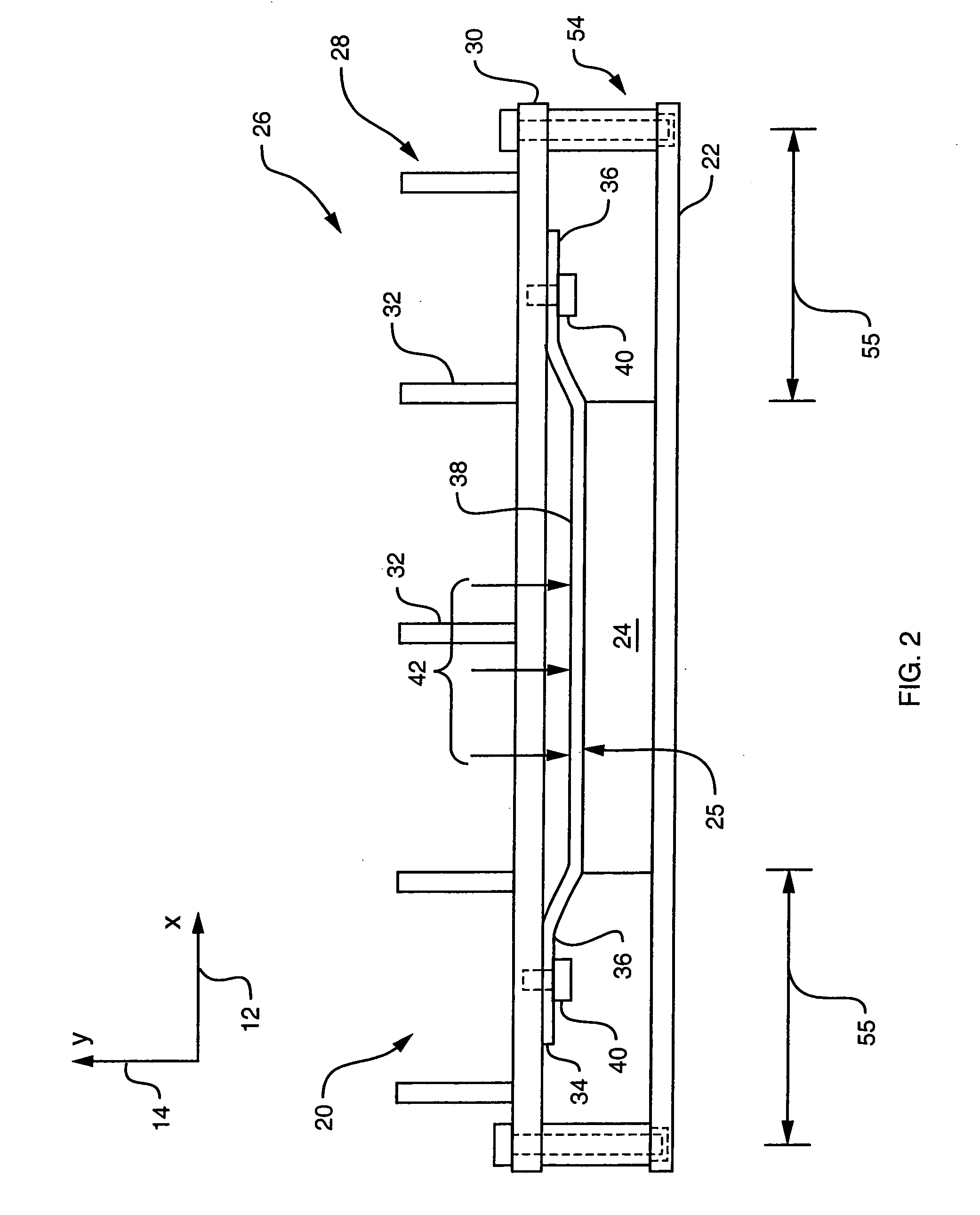
[0022]Embodiments of the present invention provide mechanisms and techniques for thermally coupling a heat sink to a circuit board component. A heat sink has a flexure member attached to a base of the heat sink and located between the base and an associated circuit board component. As the heat sink attaches to a circuit board carrying the circuit board component, the flexure member conforms to the surface of the circuit board component, thereby thermally contacting the circuit board component. The flexure member absorbs local tolerance differences on the circuit board component to provide a relatively uniform stress across the surface of the circuit board component. The flexure member also limits the amount of stress generated by the heat sink on the circuit board component when the heat sink attaches to the circuit board. When used in conjunction with a heat sink spanning several circuit board components, the flexure member absorbs global tolerance differences among the circuit boa...


PUM


Abstract

A heat sink has a flexure member attached to a base of the heat sink and located between the base and an associated circuit board component. As the heat sink attaches to a circuit board carrying the circuit board component, the flexure member conforms to the surface of the circuit board component, thereby thermally contacting the circuit board component. The flexure member absorbs local tolerance differences on the circuit board component to provide a relatively uniform stress across the surface of the circuit board component. The flexure member further limits the amount of stress generated by the heat sink on the circuit board component. When used in conjunction with a heat sink spanning several circuit board components, the flexure member absorbs global tolerance differences among the circuit board components, thereby providing relatively uniform stresses to all of the circuit board components and limiting the amount of stress experienced by any one circuit board component.

Description

BACKGROUND OF THE INVENTION[0001]A typical circuit board includes a section of circuit board material (e.g., fiberglass, copper, vias, etc.) and circuit board components that are mounted to the section of circuit board material. Examples of circuit board components include integrated circuits (ICs), resistors, and inductors. Typically, these circuit board components generate heat during operation. A fan assembly typically generates an air stream that passes over the components and carries the heat away. The air stream removes the heat so that the components do not operate in an unsafe temperature range, i.e., an excessively high temperature range that would cause the components to operate improperly (e.g., generate a signal incorrectly) or sustain damage (e.g., overheat, burnout, etc.).[0002]Some ICs include heat sinks to facilitate cooling. In general, a heat sink is a flanged metallic device that contacts a package of the IC. Certain conventional heat sinks maintain thermal contac...

Claims


Application Information

Patent Timeline
Patent Type & Authority Patents(United States)
IPC IPC(8): H05K7/20
CPCH01L23/433H01L2224/16H01L2924/01019H01L2924/01004H01L2224/73253H01L2924/00011H01L2924/00014H01L2224/0401
Inventor AHMAD, MUDASIRHUBBARD, KENNETH
Owner CISCO TECH INC
Why Eureka
Try Eureka