
Method of generating test pattern for integrated circuit

a technology of integrated circuits and test patterns, applied in the field of generating test patterns for integrated circuits, can solve the problems of interfering with the correct test, undesirable large integrated circuit b>100/b>, etc., and achieve the effect of increasing the circuit scale and preventing the noise from being generated

Inactive Publication Date: 2006-04-04
RENESAS ELECTRONICS CORP
View PDF9 Cites 3 Cited by
  • Summary
  • Abstract
  • Description
  • Claims
  • Application Information

AI Technical Summary

Benefits of technology

[0013]The present invention has been developed to solve the above described problems, and aims at providing a method of generating a test pattern for an integrated circuit capable of preventing the noise from being generated by a simultaneous change in output buffers without an increase in circuit scale.

Problems solved by technology

However, the following problem occurs if it is determined whether or not the output of “all 1” is correctly transmitted immediately after the determination as to whether or not the output of “all 0” is correctly transmitted.
Such noise as is not generated in the normal operation, but is generated by such a large electric current may produce defective test data, thereby interfering a correct test.
However, the above described conventional technology has the following problem.
As a result, the integrated circuit 100 becomes undesirably large.

Method used


Image

  • Method of generating test pattern for integrated circuit
  • Method of generating test pattern for integrated circuit
  • Method of generating test pattern for integrated circuit

Examples


first embodiment

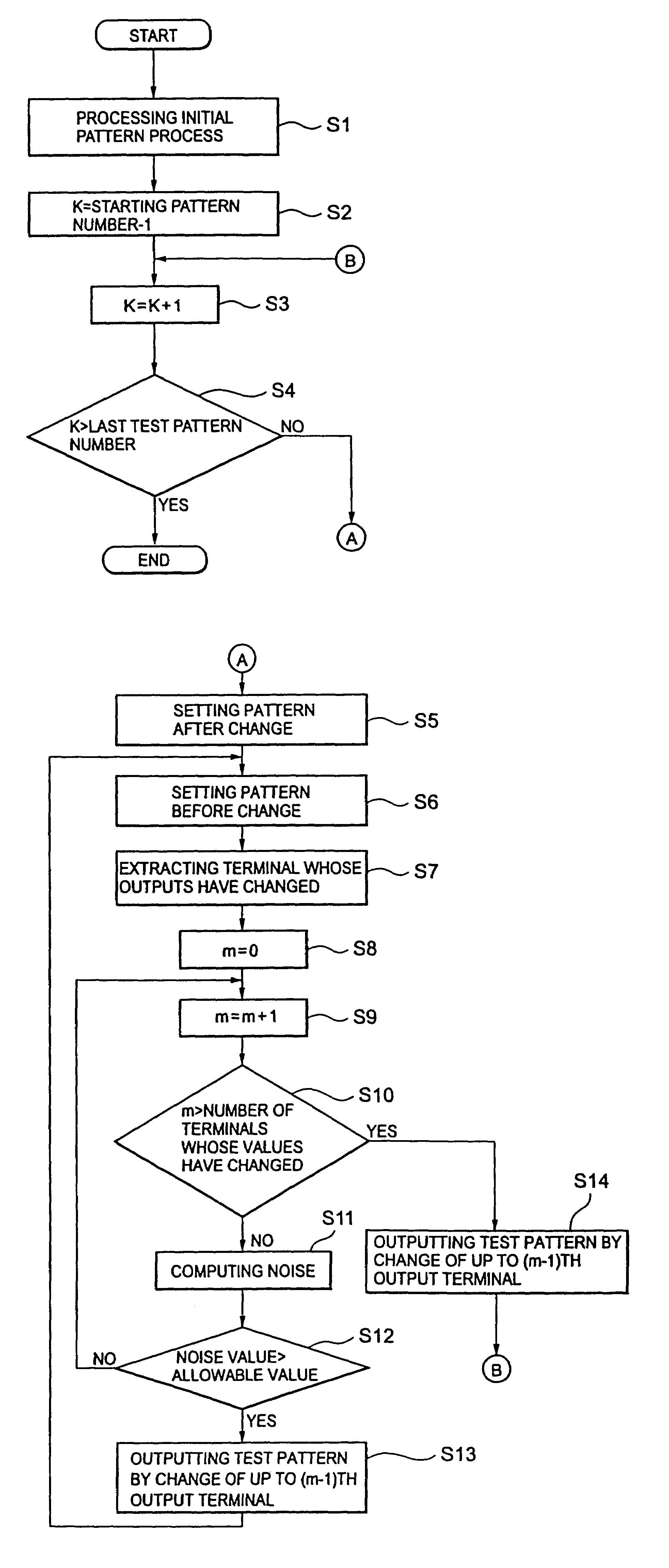
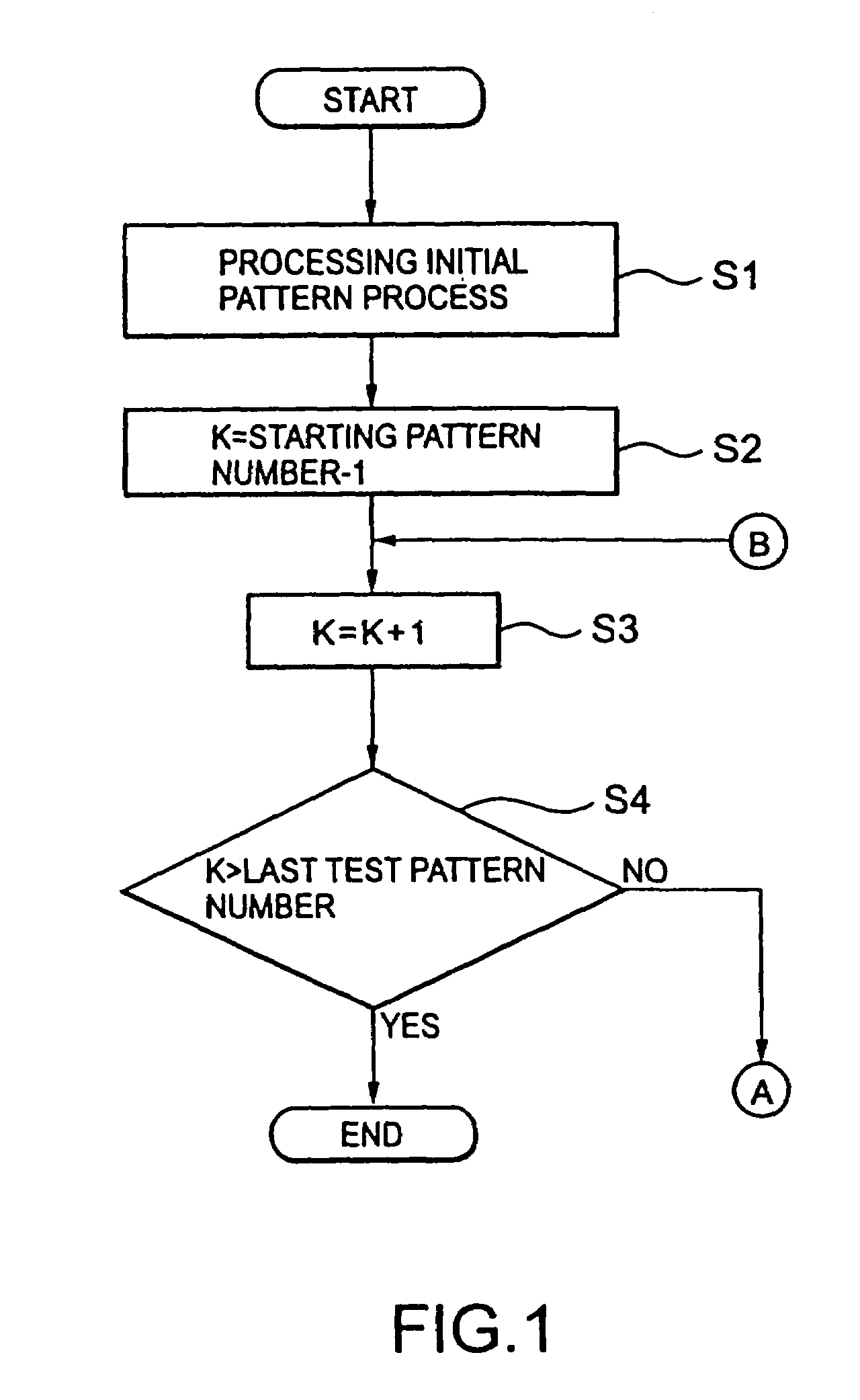
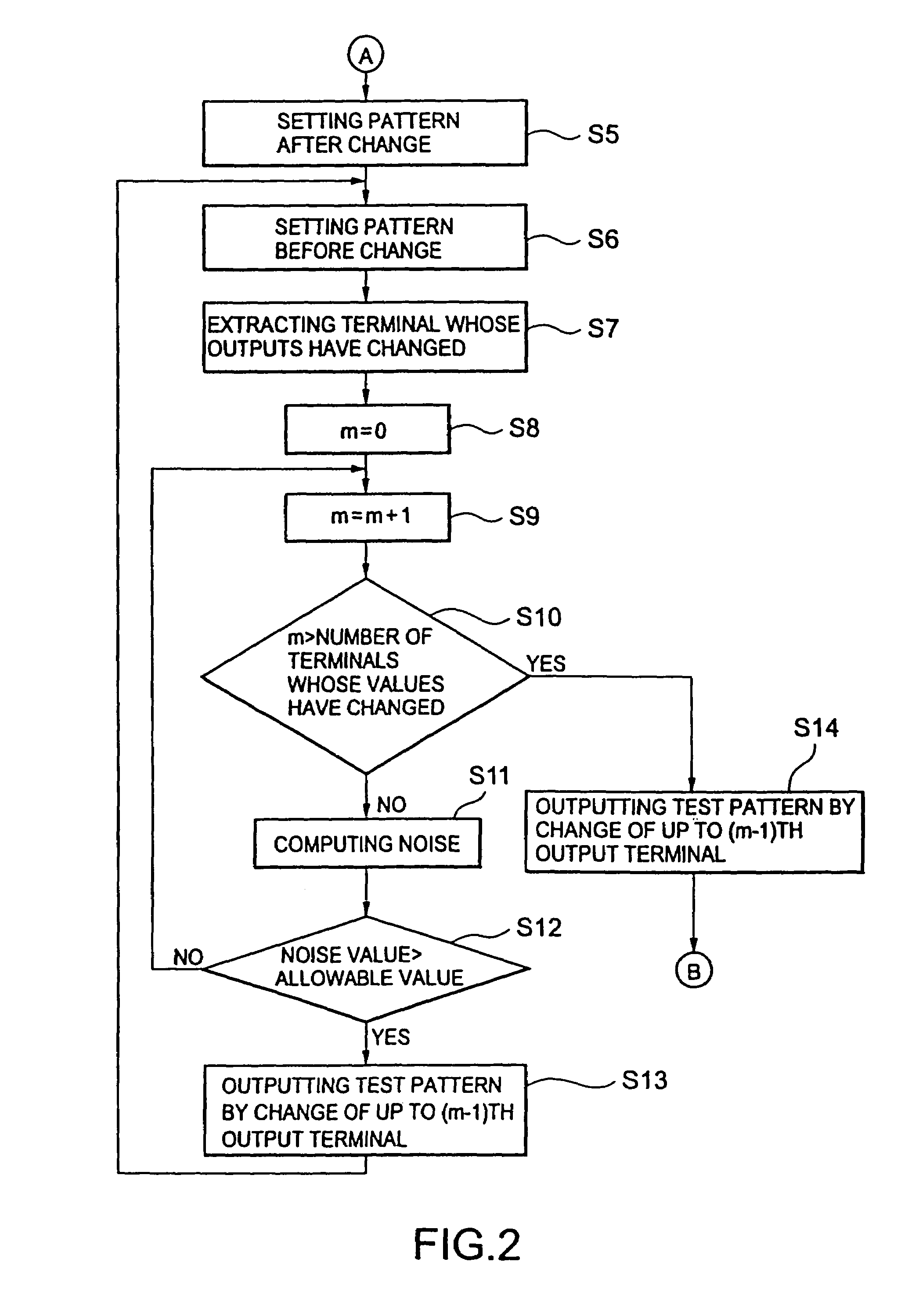
[0038]FIG. 1 is a flowchart of the method of generating a test pattern for an integrated circuit according to the first embodiment of the present invention. FIG. 2 is a flowchart of the method of generating a test pattern for the integrated circuit. FIG. 3 is a block diagram of the outline of the configuration of the simulation device for embodying the method of generating a test pattern for the integrated circuit. FIG. 4 is a block diagram of the outline of the configuration of an LSI in which a test pattern generated by the method of generating a test pattern for the integrated circuit is used. FIG. 5 is a block diagram of the outline of the configuration of the boundary scan cell in the LSI in which a test pattern generated by the method of generating a test pattern for the integrated circuit is used. FIG. 6 shows an example of a test pattern processed by the method of generating a test pattern for the integrated circuit. FIG. 7 shows an example of a test pattern generated by the...

second embodiment

[0086]Described below is the second embodiment of the present invention.

[0087]FIG. 15 is a flowchart showing a method of generating a test pattern for the integrated circuit according to the second embodiment of the present invention. FIG. 16 is a flowchart showing a method of generating a test pattern for the integrated circuit. FIG. 17 shows the grouping process in the method of generating a test pattern of the integrated circuit. FIG. 18 shows an example of a test pattern generated by the method of generating a test pattern for the integrated circuit.

[0088]Since the second embodiment is different from the first embodiment only in procedure stored in the storage unit 2, only this point will be explained here. In the procedure stored in the storage unit 2 of the embodiment, the central processing unit 3 performs the following process. That is, the central processing unit 3 groups the output terminals (step S21). Even if all output terminals in a group simultaneously change, the cen...


PUM


Abstract

A method for preventing the scale of a circuit from being extended and for preventing noise from being generated by a simultaneous value change in output buffers includes: the first process of checking the number of output buffers 15A through 15D whose output values change when boundary scan cells 13E through 13H output input patterns; the second process of checking the noise value generated by the change in the output values when all output values from the output buffers checked in the first process change; the third process of selecting the output buffer from the buffers checked in the first process such that the noise value checked in the second process can be within the noise allowable value; and the fourth process of outputting as a test pattern a pattern obtained by amending the input pattern such that the output value of the output buffer selected in the third process can change.

Description

CROSS-REFERENCE TO RELATED APPLICATION[0001]The present application is a continuation of U.S. application Ser. No. 09 / 265,346 which was filed on Mar. 9, 1999 now abandoned.BACKGROUND OF THE INVENTION[0002]1. Field of the Invention[0003]The present invention relates to a method of generating a test pattern for an integrated circuit, and more particularly to a method of generating a test pattern used in conducting a test using a boundary scan system.[0004]2. Description of the Prior Art[0005]FIG. 19 shows an example of an integrated circuit using a boundary scan system. In an integrated circuit 100 of FIG. 19, common data applied to input terminals 101A through 101D is applied to an internal circuit 104 through input buffers 102A through 102D and boundary scan cells 103A through 103D. The internal circuit 104 is a logical circuit including various gates, etc. The data from the internal circuit 104 is applied to output terminals 106A through 106D through boundary scan cells 103E throug...

Claims


Application Information

Patent Timeline
Patent Type & Authority Patents(United States)
IPC IPC(8): G01R31/28G01R31/3183G01R31/3185
CPCG01R31/318321G01R31/318547G01R31/318342G01R31/28
Inventor YAMAUCHI, HISASHI
Owner RENESAS ELECTRONICS CORP
Learn More