Semiconductor memory device for controlling output timing of data depending on frequency variation

a memory device and oscillator technology, applied in the field of synchronous memory devices, can solve the problems of data access schemes used in conventional synchronous memory devices that cannot be effectively used for input/output, data cannot be output exactly in synchronity to the rising edge and the falling edge of the external clock, and the system speed that is required for high speed operation

Inactive Publication Date: 2006-04-11
SK HYNIX INC
View PDF3 Cites 39 Cited by
  • Summary
  • Abstract
  • Description
  • Claims
  • Application Information

AI Technical Summary

Problems solved by technology

However, the SDR synchronous memory device is far from satisfying the system speed that is required for high speed operation.
However, because the DDR memory device should input / output two data in a clock cycle, the data access scheme used in the conventional synchronous memory device cannot be used for effectively performing input / output.
However, due to the delay time of the clock signal, which happens inevitably during inner processing, data cannot be outputted exactly in synchronous to the rising edge and the falling edge of the external clock.
However, as the operating frequency of the memory device increases, it gets difficult to output data at the timing scheduled by the CAS latency.
The data output timing varies depending on the operating frequency even with a same CAS latency, which makes it even difficult to output data reliably with the conventional structure in a high frequency range, e.g., over 500 Hz).

Method used


Image

  • Semiconductor memory device for controlling output timing of data depending on frequency variation
  • Semiconductor memory device for controlling output timing of data depending on frequency variation
  • Semiconductor memory device for controlling output timing of data depending on frequency variation

Examples


Embodiment Construction

[0051]Hereinafter, with reference to the accompanying drawings, a preferred embodiment of the present invention will be explained in detail.

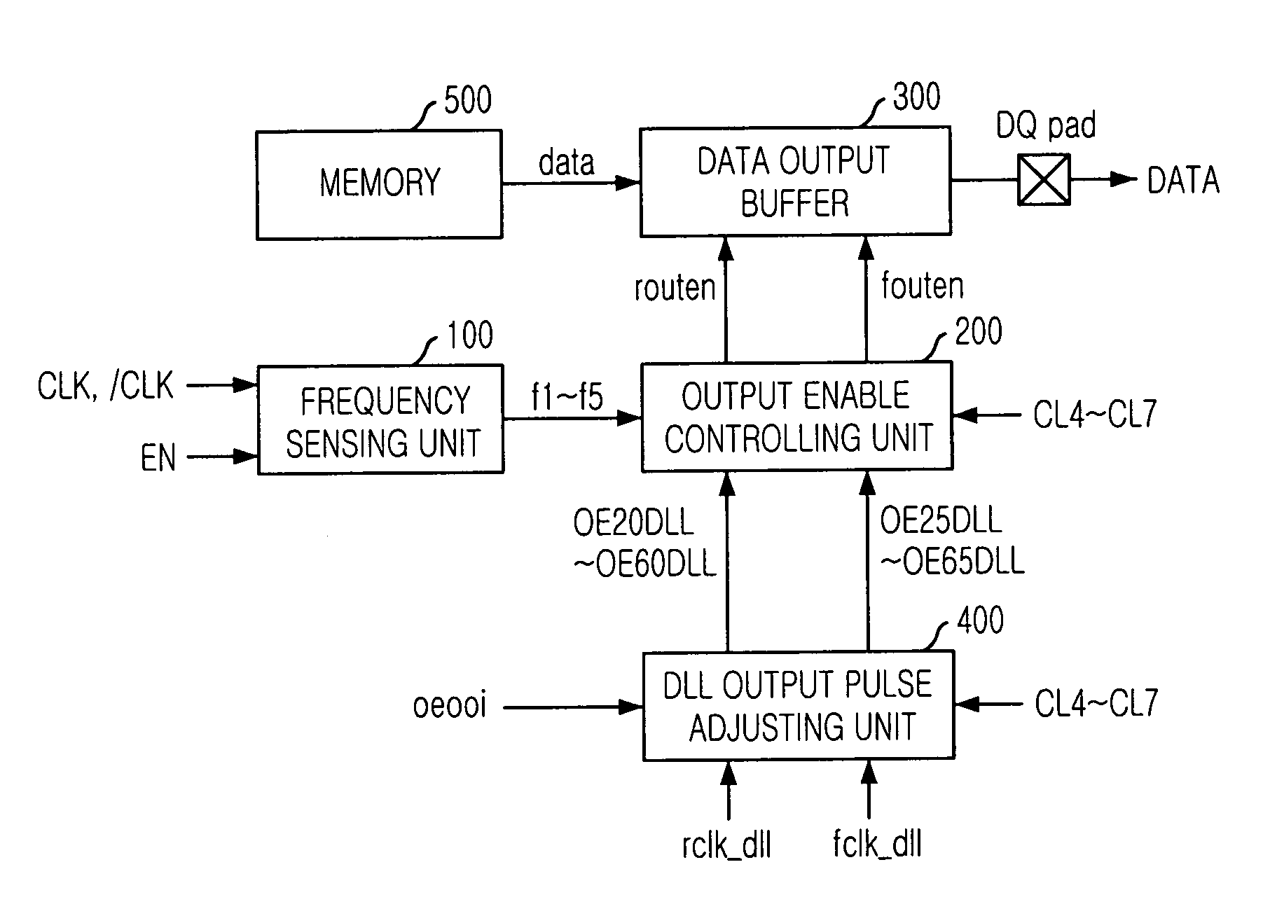
[0052]FIG. 4 exemplifies a block diagram of a semiconductor memory device in accordance with the present invention.

[0053]The semiconductor memory device of the present invention comprises a frequency sensing unit 100 for sensing an operating frequency by sensing an amount of lead of delay locked clocks rclk_dll, fclk_dll of a DLL(delay locked loop) compared to external clock signals CLK, / CLK to output corresponding signals f1–f5, an output enable controlling unit 200 for outputting output enable signals routen, fouten in response to CAS latency value CL4–CL7 with controlling the output timing of the output enable signals routen, fouten based on the frequency that is sensed by the frequency sensing unit 100, and a data output buffer 300 for outputting data that is transferred from a memory core region 500 in response to the output enable signals...


PUM


Abstract

A semiconductor memory device is capable of controlling the data output timing depending on the operating frequency so as to output data with optimized for the operating frequency. Further, in the high frequency operation, the memory device can output data reliably so as to facilitate development of high frequency memory device. The semiconductor memory device comprises a frequency sensing unit for sensing an operating frequency by sensing an amount of lead of a delay locked clock in a delay locked loop compared to an external clock signal, an output enable controlling unit for outputting an output enable signal in response to a CAS latency with controlling the output timing of the output enable signal based on the frequency that is sensed by the frequency sensing unit, and a data output buffer for outputting data that is transferred from a memory core region in response to the output enable signal.

Description

FIELD OF THE INVENTION[0001]The present invention relates to semiconductor memory devices; and, more particularly, to a synchronous memory device for controlling output timing of data depending on frequency.BACKGROUND OF THE INVENTION[0002]A semiconductor memory device has been improved for increase of its operating speed as well as its integration. For the purpose of increasing operating speed, a synchronous memory device has been introduced, which can be operated in synchronous to an external clock that is provided from outside of the memory chip.[0003]The first suggested one is, so called, a SDR(single data rate) synchronous memory device that outputs one data within a clock cycle from a data pin in synchronous to the rising edge of the external clock.[0004]However, the SDR synchronous memory device is far from satisfying the system speed that is required for high speed operation. Therefore, another one, so called, a DDR(double data rate) synchronous memory device has been sugges...

Claims


Application Information

Patent Timeline
Patent Type & Authority Patents(United States)
IPC IPC(8): G11C7/00G11C7/10H03K5/19G11C11/407H03K5/00H03K19/0175H03L7/06H03L7/081
CPCG11C7/1051H03L7/0812G11C7/1066G11C7/106G11C7/1063G11C7/20G11C7/22
Inventor LEE, HYUN-WOO
Owner SK HYNIX INC
Why Eureka
Try Eureka