

Insulated gate semiconductor device
- Summary
- Abstract
- Description
- Claims
- Application Information
AI Technical Summary
Benefits of technology
Problems solved by technology
Method used
Image

Examples
Embodiment Construction
[0040]Some embodiments of the invention will now be explained below with reference to the drawings. In FIGS. 1, 8 and 9, the same components as those of FIG. 10 are labeled with common reference numerals.
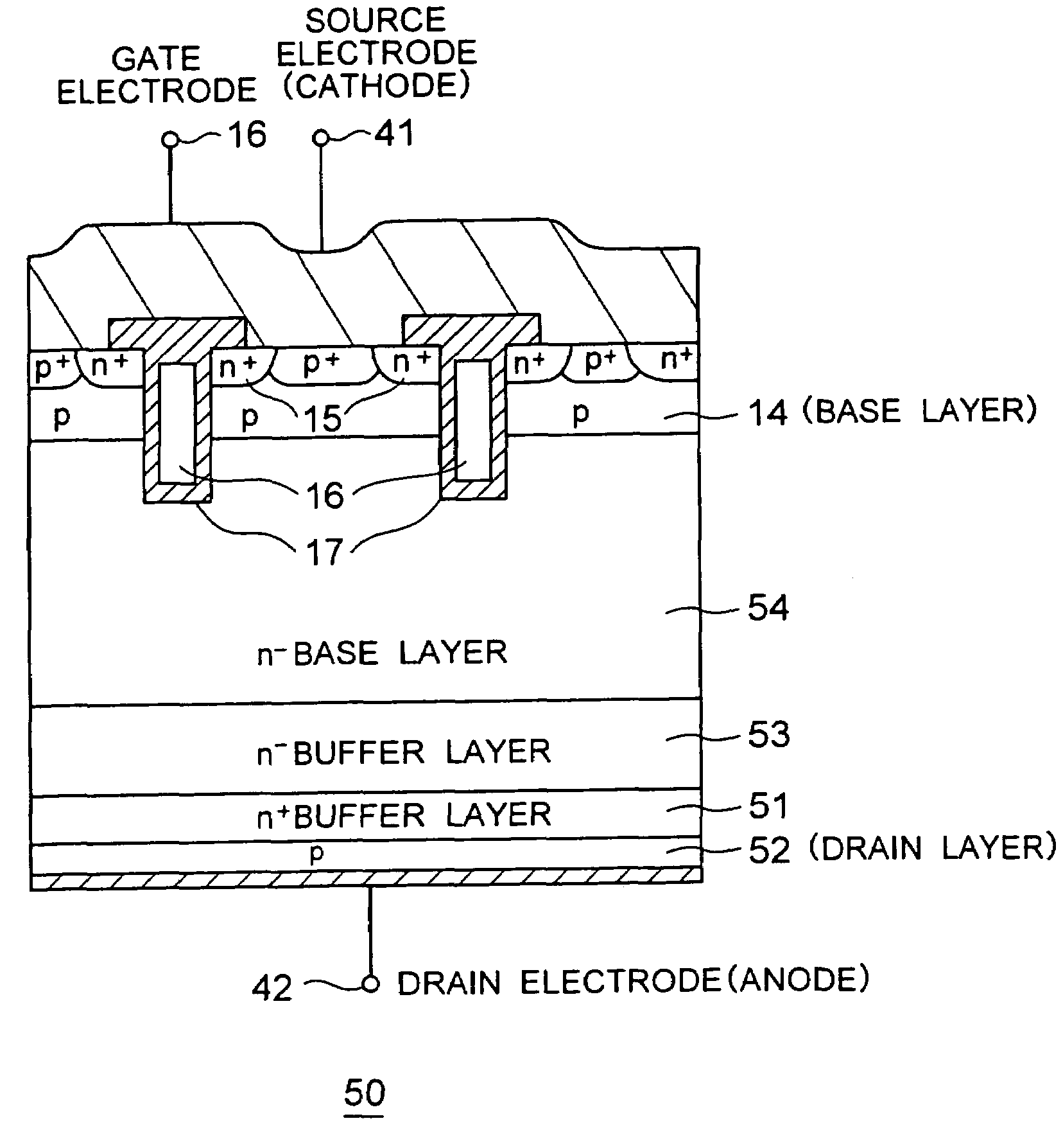
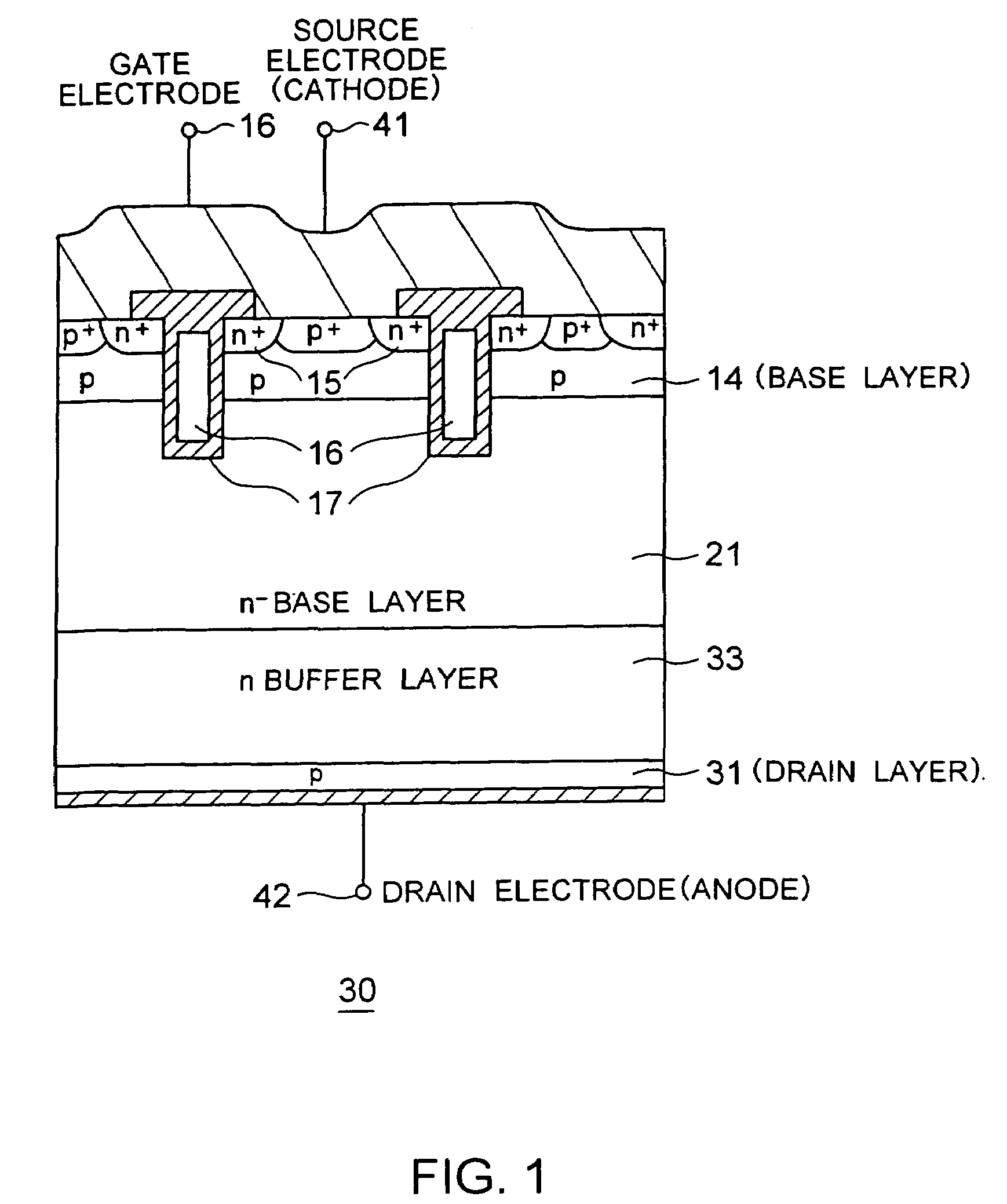
[0041]FIG. 1 is a cross-sectional view of a punch-through IGBT 30 taken as an insulated gate semiconductor device according to the first embodiment of the invention. IGBT 30 includes an n−-type base layer 21, and a p-type base layer 14 formed on the n-type base layer 21. The p-type base layer 14 includes an n+-type source layer 15 formed in a selective top surface region thereof. A p-type drain layer (anode) 31 underlies the bottom surface of the n-type base layer 21 opposite from the top surface thereof. A gate electrode 16 is formed in the n-type base layer 21 and in the p-type base layer 14 so as to make a channel in the p-type base layer 14 for electrical conduction between the source layer 15 and the n-type base layer 21. The gate electrode 16 is insulated from the n-type base ...
PUM
 Abstract
Description
Claims
Application Information