Liquid crystal display device

Active Publication Date: 2006-04-18
PANASONIC LIQUID CRYSTAL DISPLAY CO LTD +1
View PDF8 Cites 2 Cited by
  • Summary
  • Abstract
  • Description
  • Claims
  • Application Information

AI Technical Summary

Benefits of technology

[0012]Further, as shown in FIG. 24A to FIG. 24C, when one substrate in an intermediate state (FIG. 24A) is pushed (FIG. 24B), the distance between the substrate SUB1 and the substrate SUB2 is narrowed (d2<d1); and, hence, the distance between the pixel electrode PX and the counter electrode CT is narrowed.
[0050]It is another object of the present invention to provide a liquid crystal display device which will effectively utilize the above-mentioned dark spot phenomenon.
[0055]In this case, it appears preferable to apply a voltage that is equal to or less than 30% of the maximum voltage. However, since the state of the intermediate layer MIDL exists as a metastable state, the inventors have found that it is preferable to decrease the voltage which forms the electric field to a value equal to or less than 20% of the maximum voltage, so as to eliminate the metastable state.
[0056]Then, due to the decrease of the voltage, the electric field is made small, and, hence, the liquid crystal molecules in the vicinity of the interface of the intermediate layer MIDL approach the state in which such liquid crystal molecules are arranged in parallel to the liquid crystal molecules in the vicinity of the vertical orientation film, so that the intermolecular force of the liquid crystal molecules with the intermediate layer MIDL is increased.
[0059]It is more desirable to completely dissipate the ability of the electric field to maintain the intermediate layer MIDL. To this end, it is desirable to minimize the electric field, that is, to apply the minimum voltage. With this application of the minimum voltage, it is possible to recover the display in a very short time.

Problems solved by technology

Accordingly, the fact that the trace remains in the above-mentioned manner creates a serious drawback in the practical use of the display device.
This is because the liquid crystal display panel LPNL cannot produce a normal display at the location of the trace remaining portion of the display device.

Method used


Image

  • Liquid crystal display device
  • Liquid crystal display device
  • Liquid crystal display device

Examples


embodiment 1

>

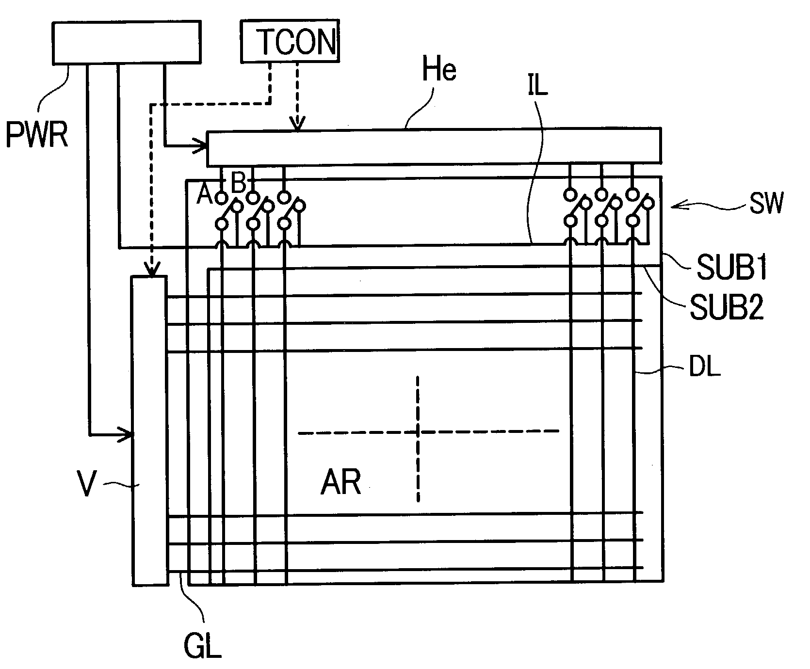
[0140]FIG. 1A is a schematic diagram showing the overall constitution of one embodiment of the liquid crystal display device according to the present invention.

[0141]In FIG. 1A, a pair of transparent substrates SUB1, SUB2 are arranged so as to face each other, with a liquid crystal material being disposed therebetween, wherein the liquid crystal material is hermetically filled in a gap defined between a pair of transparent substrates SUB1, SUB2 are sealed by means of a sealing material (not shown in the drawing), which also performs the function of fixing the transparent substrate SUB2 to the transparent substrate SUB1.

[0142]On a liquid-crystal-side surface of the above-mentioned transparent substrate SUB1, in an area surrounded by the sealing material, that are gate signal lines GL, which extend in the x direction and are arranged in parallel in the y direction, and drain signal lines DL, which extend in the y direction and are arranged in parallel in the x direction.

[0143]Regions...

embodiment 2

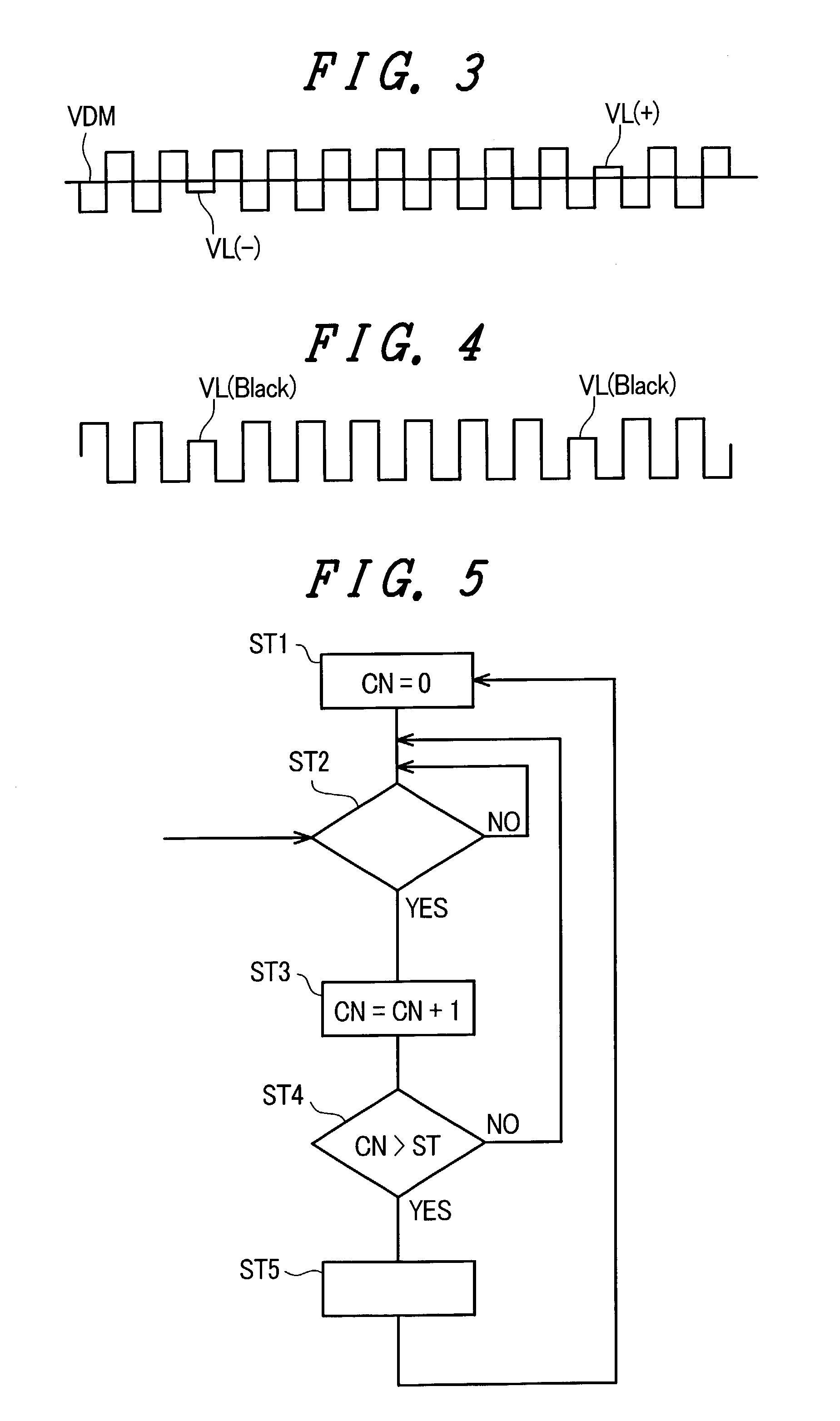
[0178]FIG. 5 is directed to an embodiment of the liquid crystal display device according to the present invention, and, more specifically, it is a flow chart showing the operation for inputting data for erasing. Operations executed in accordance with the flow chart are controlled by the above-mentioned control circuit TCON.

[0179]In FIG. 5, first of all, the counter CN is set to the state “0” in step 1 (ST1), and, thereafter, it is judged whether a synchronous signal is inputted or not in step 2 (ST2).

[0180]When the synchronous signal is inputted, 1 is added to the counter value CM in step 3 (ST3), and it is judged whether the value is greater than a set value ST or not in step 4 (ST4).

[0181]When the value is not greater than the set value, the processing returns to step 2 (ST2), and the processing waits for the inputting of the next synchronous signal.

[0182]When the value is greater than the set value, the processing replaces a video signal with data for erasing in step S (ST5), and...

embodiment 3

[0185]FIG. 7 is a view showing the manner of supplying a video signal in which the data for erasing is mixed. In FIG. 7, the data for erasing is inputted to the drain signal line DL for every 1 line, and, as a result, the data for erasing is inputted to all lines by sequentially scanning the gate signal lines GL. Here, “1 line” implies each pixel group driven by a scanning signal of one gate signal line GL.

[0186]As shown in FIG. 8, the data for erasing may be applied to the drain signal line DL for every plurality of lines. Due to such a provision, it is possible to shorten the display time of the data for erasing. In this case, the data for erasing may be displayed for a longer time.

[0187]Further, as shown in FIG. 9, the data for erasing may be simultaneously inputted to all drain signal lines DL. Due to such a provision, the display time of the data for erasing can be further shortened.


PUM


Abstract

A liquid crystal display device includes a first substrate and a second substrate, which are arranged to face each other in an opposed manner by way of liquid crystal material, first electrodes which are formed in a pixel region of a liquid-crystal-side surface of the first substrate, and second electrodes which are formed in a pixel region of a liquid-crystal-side surface of the second substrate. In such a liquid crystal display device, liquid crystal molecules are arranged in the vertical direction with respect to the substrates in a state in which an electric field is not applied between the first electrodes and the second electrodes. The liquid crystal display device, with respect to a voltage applied between the first electrodes and the second electrodes, intermittently applies a voltage which is equal to or less than 20% of the maximum voltage.

Description

BACKGROUND OF THE INVENTION[0001]The present invention relates to a liquid crystal display device; and, more particularly, to a so-called vertical orientation type liquid crystal display device.[0002]A liquid crystal display device is configured such that the optical transmissivity of a liquid crystal material in each pixel region is controlled in response to an electric field which is generated between a pair of electrodes and is applied to the liquid crystal material.[0003]In such a liquid crystal display device, orientation films are arranged so as to be directly brought into contact with the liquid crystal material, thereby to determine the initial orientation direction of the liquid crystal when an electric field is not applied to the liquid crystal.[0004]Further, although the orientation films conventionally require orientation treatment by rubbing, there is a liquid crystal mode which requires no rubbing treatment and can omit step for such a treatment, and a so-called vertic...

Claims


Application Information

Patent Timeline
IPC IPC(8): G02F1/133G02F1/139G02F1/1333G02F1/1343G06F3/041G09G3/20G09G3/36
CPCG09G3/3648G09G2320/02
Inventor KOBAYASHI, SETSUOYANAGAWA, KAZUHIKO
Owner PANASONIC LIQUID CRYSTAL DISPLAY CO LTD
Why Eureka
Try Eureka