Eureka AIR delivers breakthrough ideas for toughest innovation challenges, trusted by R&D personnel around the world.

Integrated circuit capable of locating failure process layers

a technology of integrated circuits and process layers, applied in the field of integrated circuits, can solve problems such as the vulnerability of scan chains to process variations, and achieve the effect of low yield rate and easy process finding

Inactive Publication Date: 2006-04-25
FARADAY TECH CORP
View PDF5 Cites 2 Cited by
  • Summary
  • Abstract
  • Description
  • Claims
  • Application Information

AI Technical Summary

Benefits of technology

[0007]Since the connection in the assigned routing layer is constrained to a minimum, the scan chain is vulnerable to variations in processes relevant to the assigned routing layer. This scan chain makes it easier to find processes causing low yield rate thereof.

Problems solved by technology

Since the connection in the assigned routing layer is constrained to a minimum, the scan chain is vulnerable to variations in processes relevant to the assigned routing layer.

Method used


Image

  • Integrated circuit capable of locating failure process layers
  • Integrated circuit capable of locating failure process layers
  • Integrated circuit capable of locating failure process layers

Examples


first embodiment

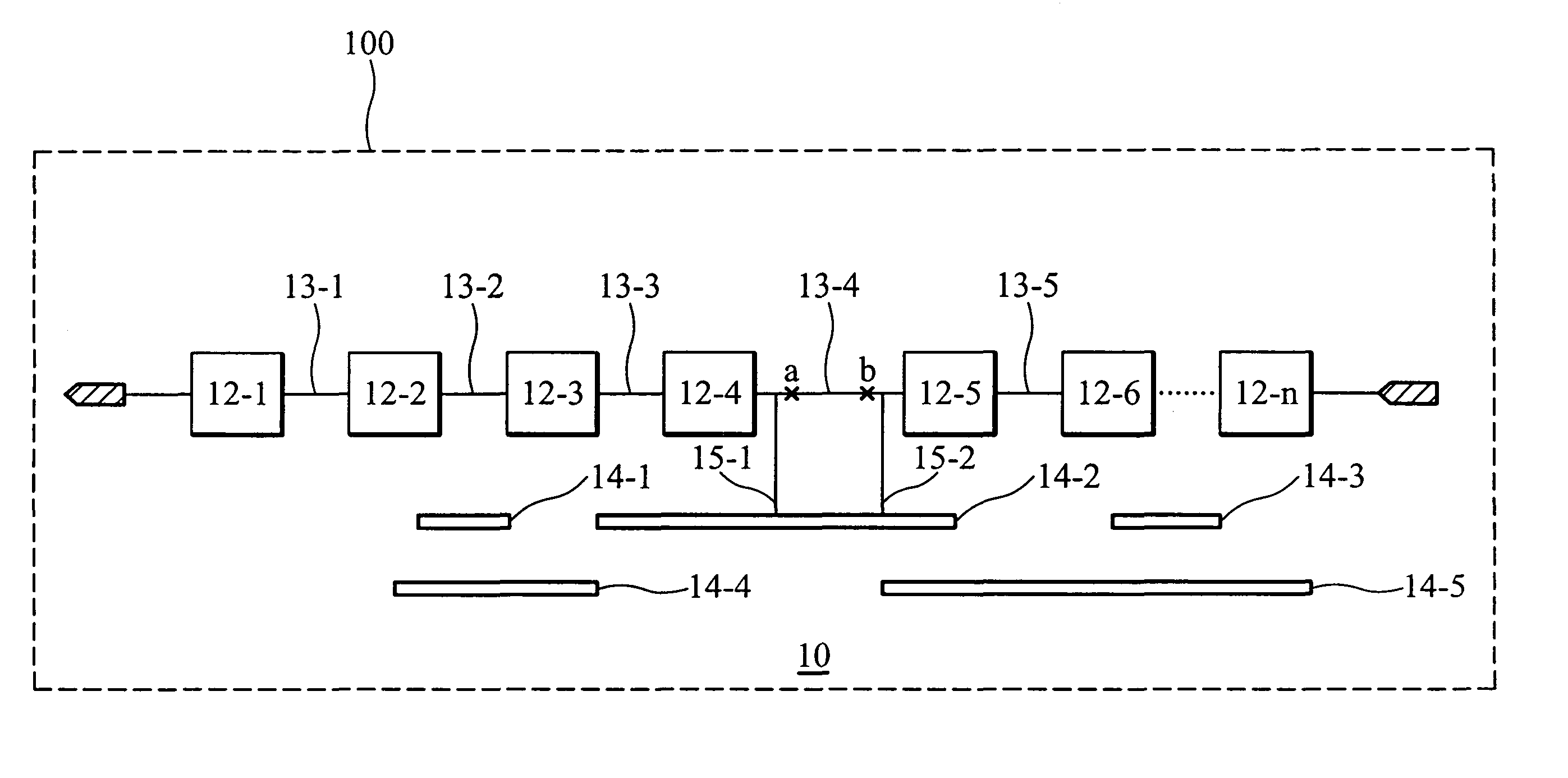
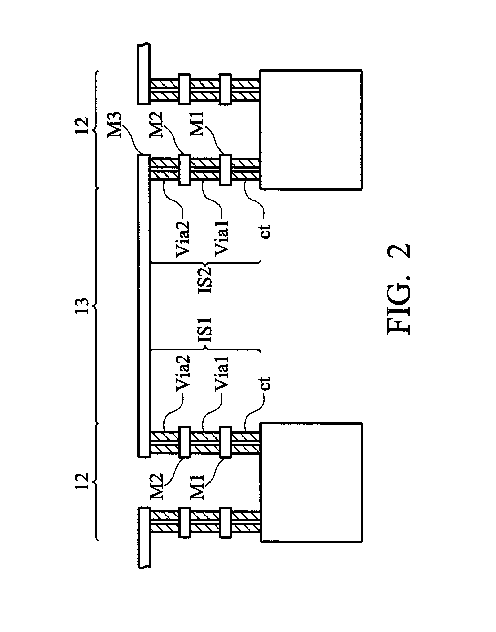
[0019]FIG. 2 shows an example of a portion of the scan chain in FIG. 1, illustrating a connection 13 between two scan cells 12. Each connection 13 between each two scan cells is formed according to a layout constraint limiting each connection 13 between each two scan cells 12 to pass through only metal 3 layer (M3), as shown in FIG. 2. In other words, connection 13 is only composed of a metal line in M3. According to the influence of processes relative to forming the M3 layer, the layout constraint also limits the width of metal line of M3 to no exceeding critical dimension (CD) of M3, as provided by the semiconductor manufacturer. Violation of design rules renders low yield and is thus not acceptable. A line with a width of CD implies that this line can easily be broken or disconnected due to process variation.

[0020]In this case, each of the first and second interconnect structures (IS1 and IS2) is composed of two conductive layers M1 and M2 and plug layers contact (ct), Via1 and V...

second embodiment

[0023]Difficulty in placement and routing may occur if each connection between two scan cells is constrained to formation by only one single metal layer. More flexibility for the layout constraint is acceptable to achieve the purpose of the invention of the present invention.

[0024]FIG. 3 is a diagram illustrating the second embodiment of scan chain 10 according to'the present invention. Not only a single metal layer but also a plurality of metal layers can be assigned and limited in the layout constraint for a scan chain. The layout constraint for a scan chain in FIG. 3 limits each connection between two scan cells to passing through only M2, M3, or Via2 and the metal lines in the connection to line width of only CD of M2 or M3. Such a layout constraint limits line formation in M2 or M3 the most likely causes of disconnection in the scan chain. To exclude failure possibility in other layers, other further layout constraints can be included to guarantee robust connection. A layout co...

third embodiment

[0025]The yield impact for processes relevant to a plug layer can also be monitored.

[0026]FIG. 4 is a diagram illustrating the third embodiment of scan chain 10 according to the present invention. The layout constraint for the scan chain in FIG. 3 limits each connection between two scan cells to passing through only M1, M2 or Via1, and, in the connection, a metal line of M1 and a metal line of M2 to connection by a single plug with a minimum diameter. To exclude failure possibility in layers other than Via1, other further layout constraints can be included to guarantee robust connection. A layout constraint for robust connection can be, for example, prohibition of forming a single plug of Contact to link a line of M1 and a stripe in Diffusion or of forming a metal line with a width of CD in all metal layers, as shown in FIG. 4. As is self-explanatory by referencing the previous embodiments, such a scan chain in FIG. 4 is vulnerable to defect or process variation during formation of ...


PUM


Abstract

An integrated circuit for locating failure process layers. The circuit has a substrate with a scan chain disposed therein, having scan cells connected to form a series chain. Each connection is formed according to a layout constraint of a minimum dimension provided by design rules for an assigned routing layer. Since the connection in the assigned routing layer is constrained to a minimum, the scan chain is vulnerable to variations in processes relevant to the assigned routing layer. The scan chain makes it easier to locate processes causing low yield rate of the scan chain.

Description

BACKGROUND OF THE INVENTION[0001]1. Field of the Invention[0002]The present invention relates to an integrated circuit, and more particularly, to an integrated circuit capable of locating failure process layers on a chip.[0003]2. Description of the Related Art[0004]For logic process debugging, memory and FPGA are usually selected. Fault isolation can be achieved through a simple bit mapping process, and further, fault isolation to locate appropriate failure process layers is also possible using the bit map signature. However, fabless ASIC companies do not have such kind of products for new process debugging and yield learning, resulting in a long learning curve for yield enhancement. Further, fabless ASIC companies must cooperate with foundry fabs closely for process debugging or development, for example accepting products on wafers having passed WAT (wafer acceptance test) of foundry fab. Unfortunately, products sometimes still experience poor yield caused by process problems. Fabl...

Claims


Application Information

Patent Timeline
Patent Type & Authority Patents(United States)
IPC IPC(8): G06F17/50G01R31/3185
CPCG01R31/31855G01R31/318538
Inventor CHENG, AN-RU ANDREWLIN, CHANG-SONGLIU, TZU-CHUNTSENG, HUAN-YUNG
Owner FARADAY TECH CORP
Why Eureka
Eureka Blog
Learn More