Electronic device sealed under vacuum containing a getter and method of operation

a technology of electronic devices and getters, applied in the field of electronic devices, can solve the problems of increasing the difficulty of assembly, and increasing the volume of the packag

Inactive Publication Date: 2006-05-09
SAMSUNG ELECTRONICS CO LTD
View PDF22 Cites 14 Cited by
  • Summary
  • Abstract
  • Description
  • Claims
  • Application Information

AI Technical Summary

Problems solved by technology

One of the major problems with vacuum packaging of electronic devices is the continuous outgassing of hydrogen, water vapor, and other components found in ambient air from the internal components of the electronic device.
At these temperatures both active devices as well as polymeric materials will be damaged and / or deformed.
In order to avoid these damaging effects the getter material must be kept apart from the actual device, thus leading to a bulkier package as well as greater difficulty in assembly.
In addition, the incorporation of a separate cartridge, especially for small electronic devices with narrow vacuum gaps, also results in a bulkier package.
Further, the utilization of a separate cartridge increases the cost of manufacturing because it is a separate part that requires accurate positioning and then it must be secured to another component part to prevent it from coming loose.
Loose cartridges are a potential serious problem by either acting as a source of small particles that break away from the cartridge or create particles from materials the cartridge is in contact with.

Method used


Image

  • Electronic device sealed under vacuum containing a getter and method of operation
  • Electronic device sealed under vacuum containing a getter and method of operation
  • Electronic device sealed under vacuum containing a getter and method of operation

Examples


Embodiment Construction

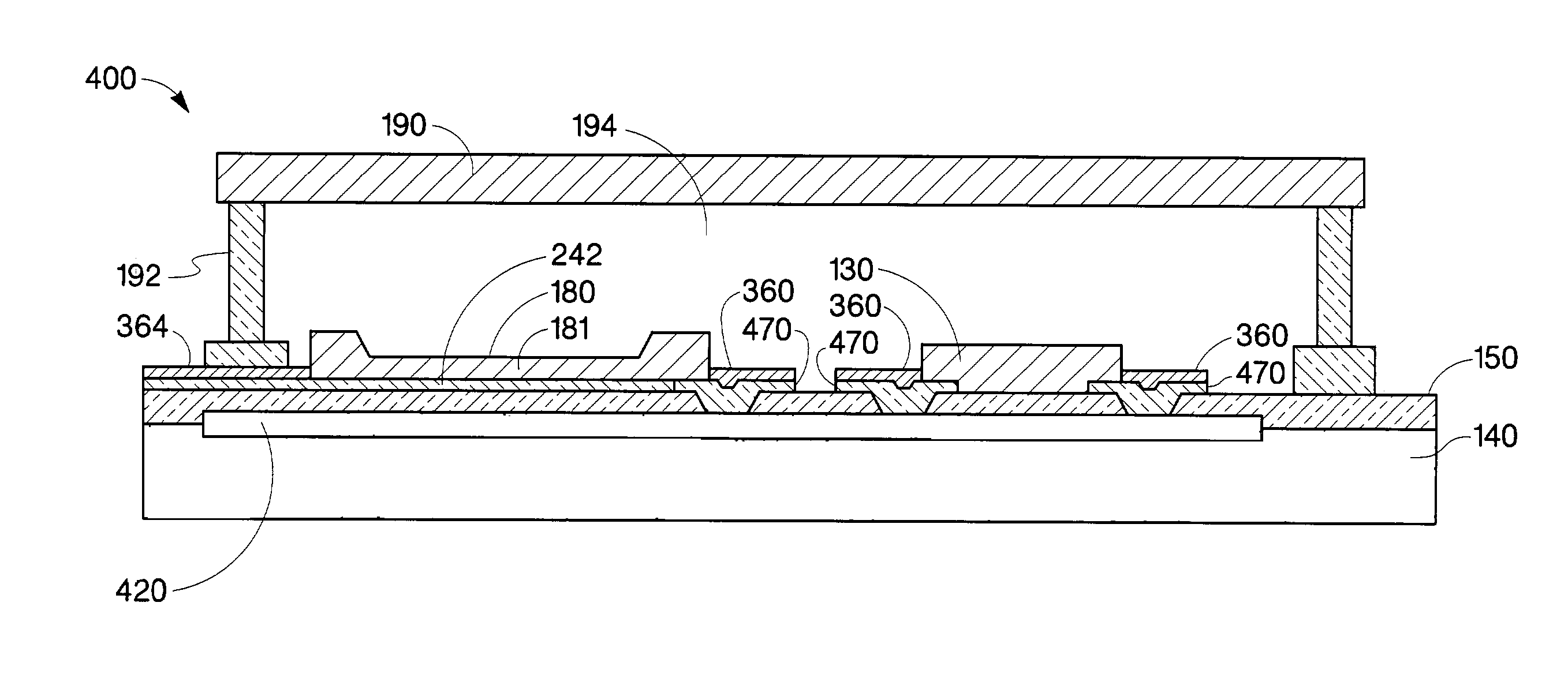
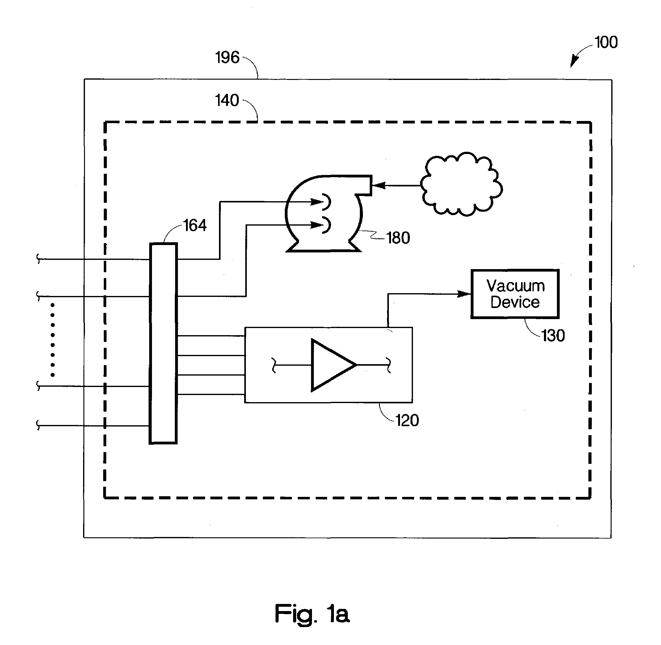
[0020]FIG. 1a is a block diagram of an electronic device sealed and maintained under vacuum, according to an embodiment of this invention. This device is referred to as electronic device 100 utilizing non-evaporable getter pump 180 (hereinafter NEG pump 180) to assist in evacuation, sealing, and maintenance of the vacuum during operation. Electronic device 100 includes the integration of NEG pump 180, vacuum device 130, and transistors 120 onto substrate 140 enclosed in package 196 that is vacuum-sealed. Vacuum device 130 relates to any electronic device that requires a vacuum to operate such as a charged particle emitter (e.g. electron or ion). Bond pads 164 are also affixed to substrate 140 providing electrical input and output. In this embodiment, there is a direct electrical connection between bond pads 164 and NEG pump 180; thus, this embodiment is commonly referred to as direct drive. NEG pump 180 includes non-evaporable getter material 181 (hereinafter NEG material 181) as sh...


PUM


Abstract

An electronic device that is sealed under vacuum includes a substrate, a transistor formed on the substrate, and a dielectric layer covering at least a portion of the transistor. The electronic device further includes a layer of non-evaporable getter material disposed on a portion of the dielectric layer; and a vacuum device disposed on a portion of the substrate. Electrical power pulses activate the non-evaporable getter material.

Description

CROSS REFERENCE TO RELATED APPLICATION(S)[0001]This is a continuation of copending application Ser. No. 09 / 836,061 filed on Apr. 16, 2001, now U.S. Pat. No. 6,534,850, which is hereby incorporated by reference herein.FIELD OF THE INVENTION[0002]This invention relates generally to electronic devices that incorporate a vacuum packaged microelectronic device. More particularly, the present invention relates to an electronic device having a non-evaporable getter material disposed on the same substrate as the active transistors and other logic devices.BACKGROUND OF THE INVENTION[0003]The ability to maintain a vacuum for a prolonged period in a microelectronic package is increasingly being sought in such diverse areas as field emission displays (FEDs), micro-electro-mechanical systems (MEMS) and atomic resolution storage devices (ARS) that are used in connection with computers, displays, television sets as a few examples. Both FEDs and ARS typically require two surfaces juxtaposed to one ...

Claims


Application Information

Patent Timeline
Patent Type & Authority Patents(United States)
IPC IPC(8): H01L23/29H01L21/44H01L21/48H01L21/50H01L23/06B81B7/00H01J7/18H01J29/94H01L23/26
CPCB81B7/0038H01J29/94H01L23/26H01J2329/00H01L2924/0002H01L2924/13091H01L2924/00
Inventor LIEBESKIND, JOHN
Owner SAMSUNG ELECTRONICS CO LTD
Why Eureka
Try Eureka