Nanometer scale data storage device and associated positioning system

a data storage device and scale technology, applied in the field of nanometer scale data storage devices and their associated positioning systems, can solve the problems of limited storage capacity of this data storage device, bulky positioning apparatus, and significant problems of data storage devices, and achieve the effect of lowering the write tip and lowering the tip

Inactive Publication Date: 2006-05-09
TERRASPAN
View PDF173 Cites 22 Cited by
  • Summary
  • Abstract
  • Description
  • Claims
  • Application Information

AI Technical Summary

Problems solved by technology

However, these data storage devices all suffer from significant problems.
This positioning apparatus is bulky and impractical to use as a part of a data storage device in a computing system.
Moreover, since positioning of the STM probes over the storage medium in the X and Y directions is limited to the range of movement of the X and Y piezoelectric translator elements of the positioning apparatus, the storage capacity of this data storage device is also limited by this range of movement.
This unfortunately increases the overall size, read / write times, weight, and power requirements of the data storage device.
However, the STM probes comprise a soft conductive material, such as conductive silicon, tungsten, aluminum, or gold which wears down after prolonged use in deforming the storage medium.
Thus, the useful life of this type of data storage device is limited.

Method used


Image

  • Nanometer scale data storage device and associated positioning system
  • Nanometer scale data storage device and associated positioning system
  • Nanometer scale data storage device and associated positioning system

Examples


Embodiment Construction

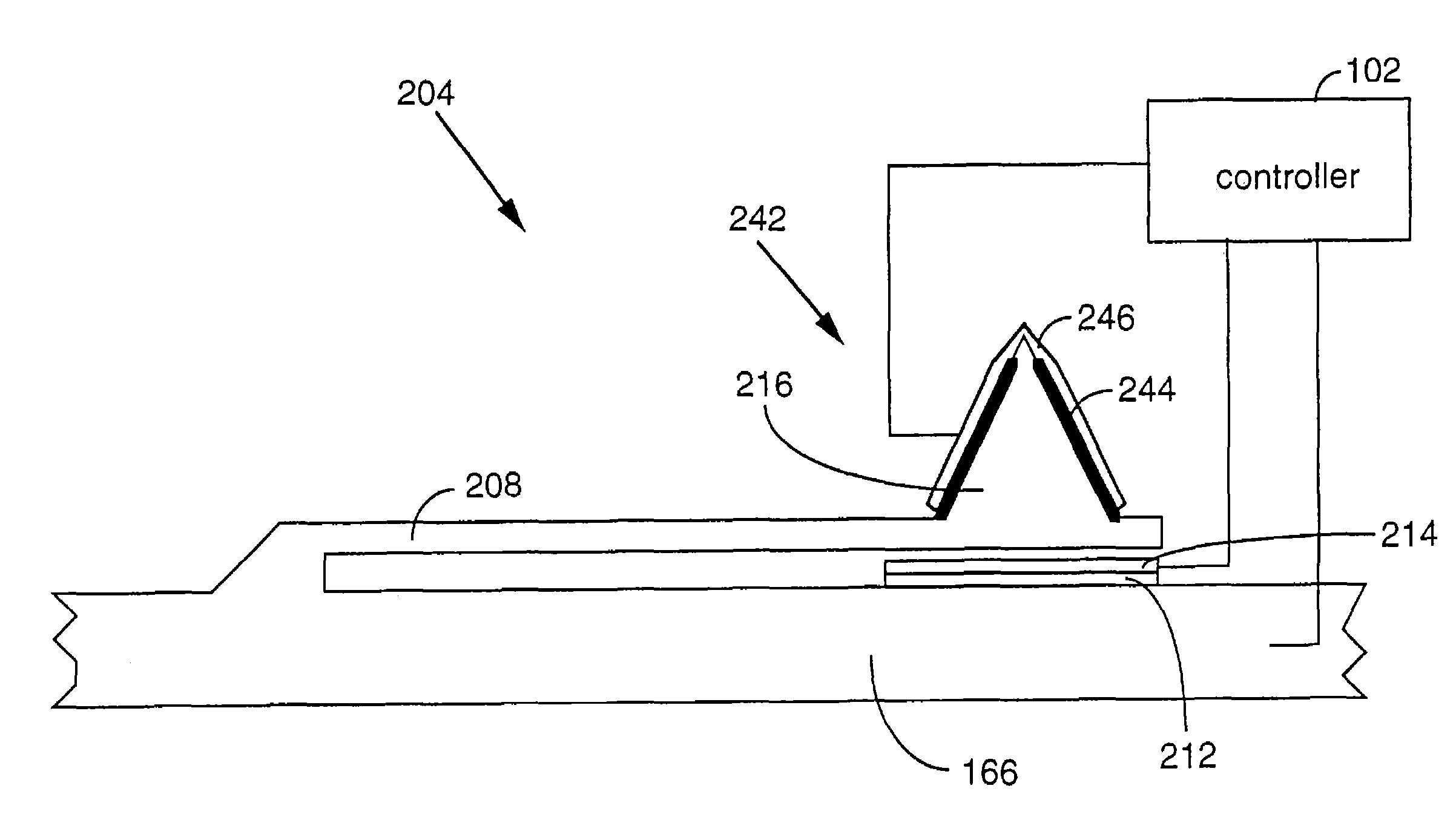
[0039]The present invention primarily concerns various types of data storage systems. These data storage systems are related by their positioning systems, storage mediums, and / or read / write mechanisms.

Positioning System

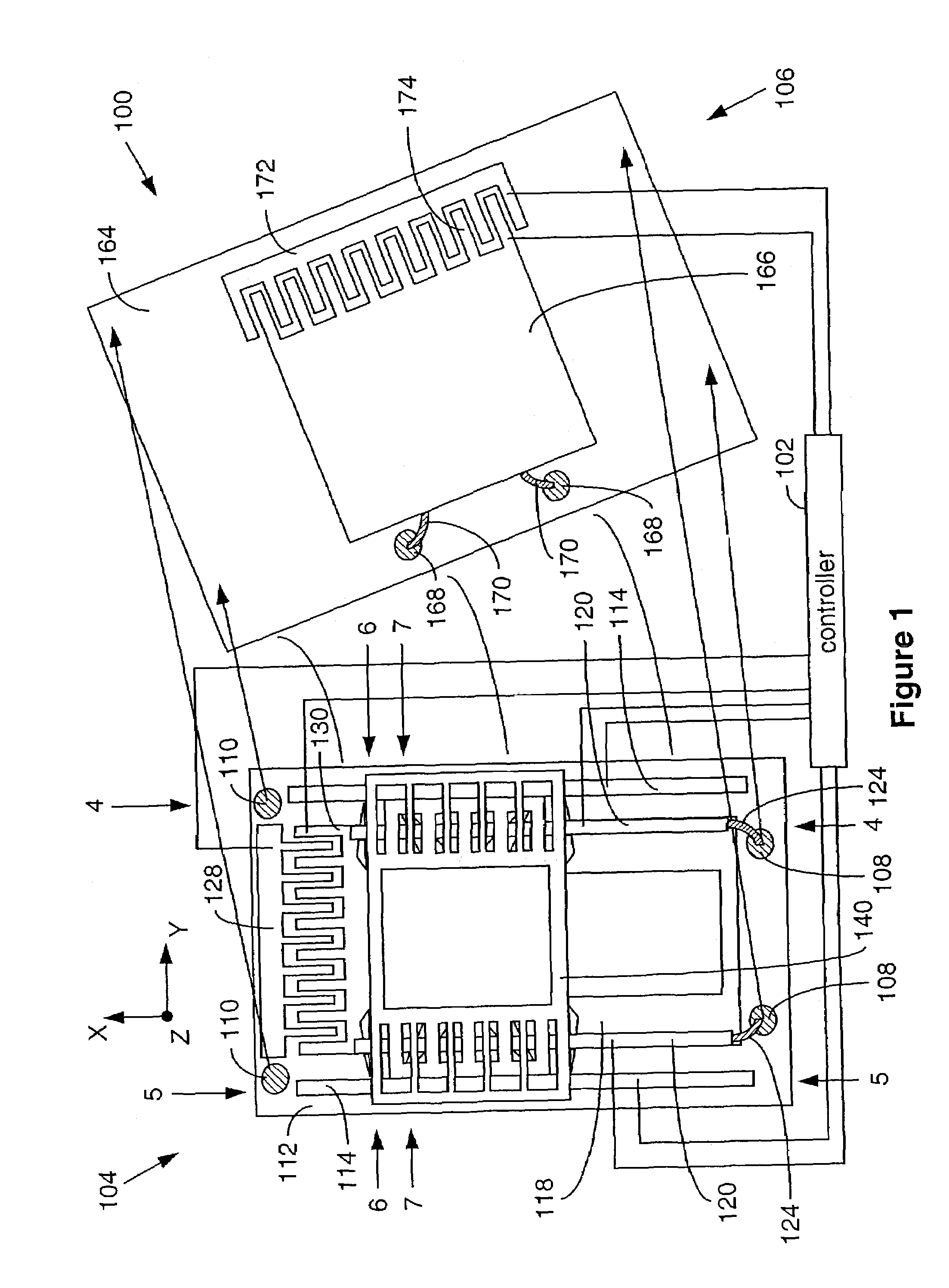
[0040]Referring to FIG. 1, there is shown a positioning system 100 for positioning objects at nanometer level or scale increments. As will be more evident from the following discussions, the positioning system may be used as the positioning system in the data storage devices described herein or as the positioning system in measuring systems (such as atomic force microscopes (AFMs), scanning tunneling microscopes (STMs), optical microscopes, and near-field microscopes), microfabrication systems, or other instruments that require precise positioning.

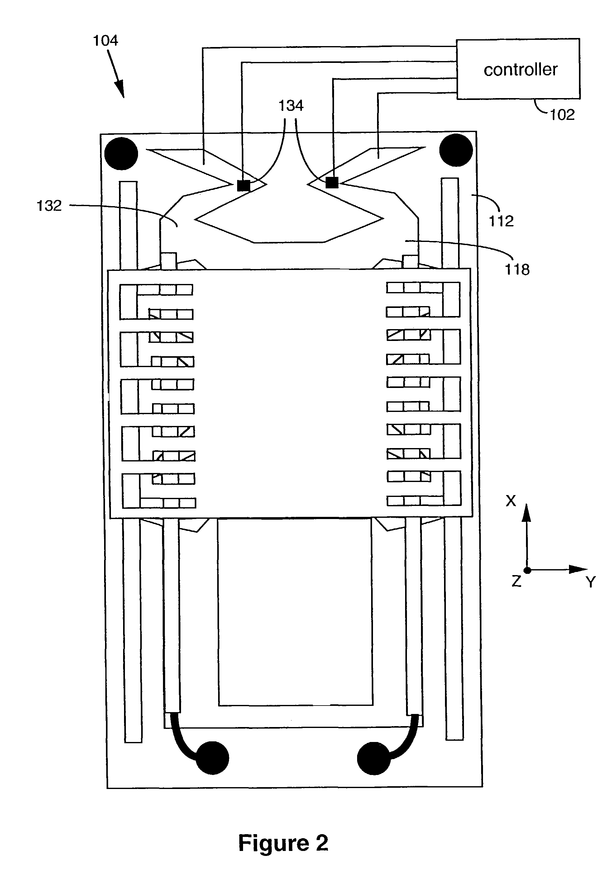
[0041]Positioning system 100 includes a programmed controller 102 and a microfabricated XY translator or positioning apparatus comprising an X translator assembly 104 to move an object in the X direction and a Y translator a...


PUM

PropertyMeasurementUnit
thicknessaaaaaaaaaa
thicknessaaaaaaaaaa
thicknessaaaaaaaaaa

Abstract

A data storage system that includes a positioning system for positioning the write / read mechanism and the storage medium of the data storage device with respect to each other in first and second predefined directions. The positioning system comprises a positioning apparatus comprising microfabricated first and second positioning assemblies. The positioning system further comprises a controller to position a positionable support structure of the first positioning assembly in a first predefined direction within a range of positioning that is larger, than the range of movement of a moveable support structure of the first positioning assembly by controlling (A) a stationary support structure clamp in clamping and unclamping the positionable structure to and from the support structure, (B) a moveable structure clamp in clamping and unclamping the positionable support structure to and from the moveable support structure, and (C) the movement of the moveable support structure. In one embodiment, one of the write / read mechanism and the storage medium is carried by the positionable support structure so that it is positioned with the first positioning assembly. The other one of the write / read mechanism and the storage medium is positioned with the second positioning assembly. In another embodiment, the positionable support structure carries the second positioning assembly and one of the write / read mechanism and the storage medium is positioned with the second positioning assembly while the other is held stationary.

Description

CROSS-REFERENCES TO RELATED APPLICATIONS[0001]This application is a continuation of U.S. patent application Ser. No. 08 / 955,031, filed Oct. 21, 1997 now U.S. Pat. No. 6,724,712, which is a division of U.S. patent application Ser. No. 08 / 506,516, filed Jul. 24, 1995, now U.S. Pat. No. 5,751,683.[0002]All of the identified and cross-referenced applications are hereby incorporated by reference in their entirety.FIELD OF THE INVENTION[0003]The present invention relates generally to data storage devices and their associated positioning systems. In particular, it relates to data storage devices to store and recover data by producing optical, electrical, or mechanical changes in storage media at nanometer level (i.e., scale) increments (i.e., intervals) with microfabricated structures which are positionable at nanometer level increments with the positioning system of the data storage devices.BACKGROUND OF THE INVENTION[0004]UV erasable programmable read only memories (UVPROMs) are well kno...

Claims


Application Information

Patent Timeline
Patent Type & Authority Patents(United States)
IPC IPC(8): G11B7/00G01B7/31G01Q30/00G01Q60/10G01Q60/18G01Q60/58G01Q70/00G03F1/84G03F7/20G11B5/00G11B5/23G11B5/31G11B9/00G11B11/12G11B11/16H02N1/00
CPCB82Y10/00G01B7/31G03F1/84G03F7/70375G03F7/70483G11B9/14G11B9/1409G11B9/1418G11B9/1427G11B9/1436G11B9/1445G11B9/1454G11B9/149G11B11/007G11B11/05H02N1/006Y10S977/877G11B5/232G11B5/3116G11B9/06G11B9/08G11B11/12G11B11/16G11B2005/0002G11B2005/0021G01Q80/00Y10S977/851Y10S977/86Y10S977/875B82Y20/00
Inventor KLEY, VICTOR B.
Owner TERRASPAN
Why Eureka
Try Eureka