Semiconductor integrated circuit device and contactless IC card

a technology of integrated circuit device and contactless interface, which is applied in the field of semiconductor integrated circuit device and contactless ic card, can solve the problem of becoming difficult to extend the communication distance between the ic card and the interrogator in operation via the contactless interfa

Active Publication Date: 2006-05-16
RENESAS ELECTRONICS CORP
View PDF12 Cites 11 Cited by
  • Summary
  • Abstract
  • Description
  • Claims
  • Application Information

AI Technical Summary

Benefits of technology

[0017]In other words, this means that the increased current across the power supply load increases the charge on the capacitor between the power supply terminals, which is provided to reduce a ripple in the voltage between the power supply terminals, and, in consequence, a high frequency component is removed from an ASK signal which corresponds to the data transmitted from the interrogator.
[0020]The object of the present invention is to provide a semiconductor integrated circuit device and a contactless IC card having a receiver circuit that enables stable demodulation of ASK-modulated signals radioed from the interrogator without being affected by other functions and the consumption current of a circuit included in the IC card and the capacitor or the like provided between the power supply terminals.

Problems solved by technology

In consequence, it is becoming difficult to extend the communication distance between the IC card and the interrogator in operation via the contactless interface.

Method used


Image

  • Semiconductor integrated circuit device and contactless IC card
  • Semiconductor integrated circuit device and contactless IC card
  • Semiconductor integrated circuit device and contactless IC card

Examples


embodiment 1

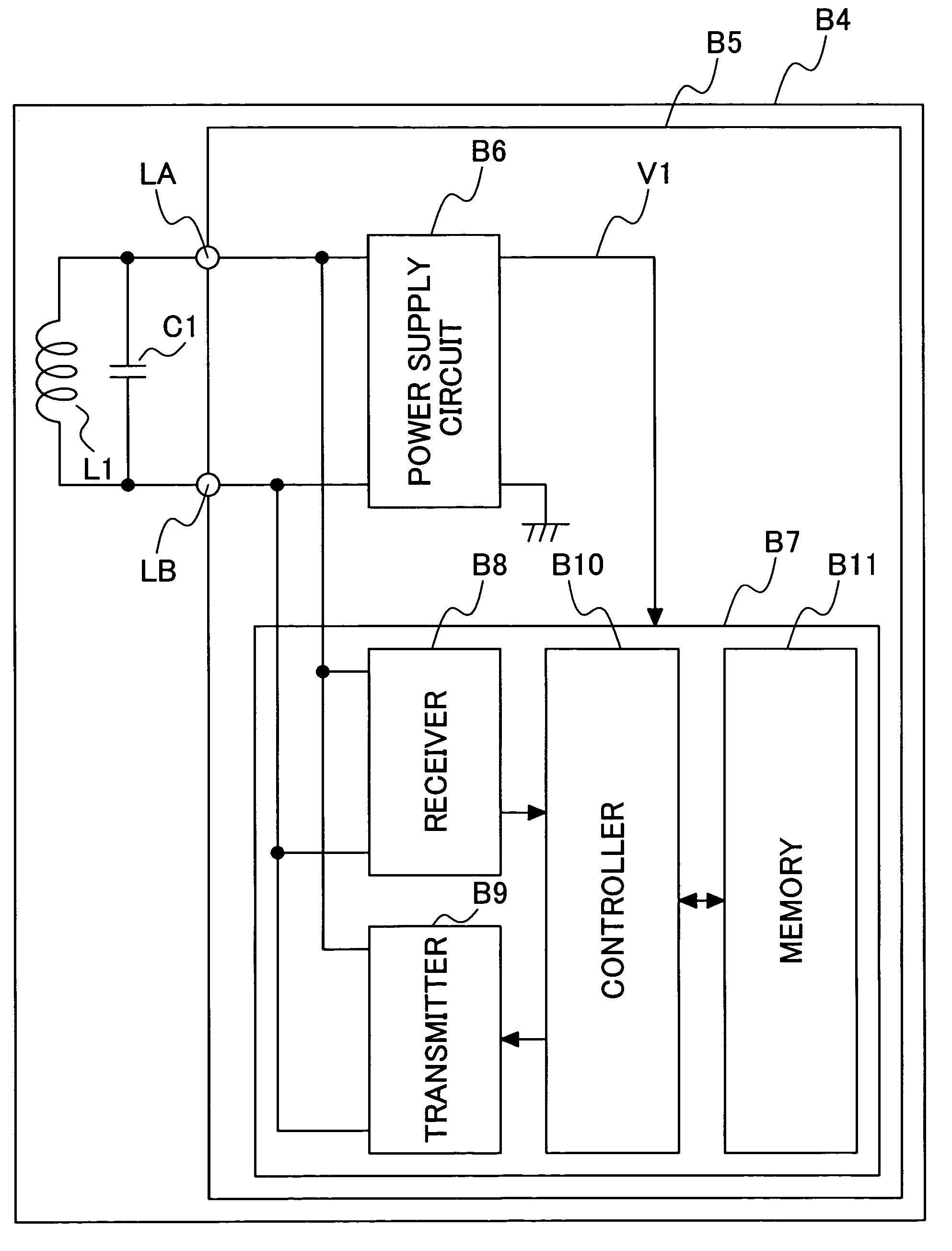
[0039]FIG. 4 is a block diagram showing a basic structure of a first embodiment of the semiconductor integrated circuit device and contactless IC card according to the present invention. In FIG. 4, the contactless IC card is identified by B4 and the semiconductor integrated circuit device and the antenna are identified by B5 and L1 respectively, which are mounted on the IC card B4. The antenna L1 and a capacitor C1 connected in parallel with the antenna L1 constitute a resonance circuit. The semiconductor integrated circuit device B5 is configured with a power supply circuit B6, an internal circuit B7, and antenna terminals LA and LB for the connections of the lines from the antennal L1.

[0040]FIG. 5 shows the structure of the IC card B4. The card form of the IC card B4 is given by a resin mold printed wiring board T1. The antenna L1 that receives electromagnetic waves from an external interrogator T4 is constructed in a spiral coil T2 formed by wiring on the printed wiring board T1....

embodiment 2

[0057]FIG. 8 is a circuit diagram showing another configuration of the feedback path which is a constituent of the receiver circuit in the semiconductor integrated circuit device discussed in Embodiment 1. The feedback path of this embodiment is configured such that two chains of diodes are connected in parallel and oriented in mutually reverse directions, and in each chain, a plurality of diodes are connected in series. In FIG. 8, by way of example, two diode chains, in one of which two diodes D7 and D8 are connected in series, and in the other of which two diodes D9 and D10 are connected in series, are connected in parallel and oriented in reverse directions.

[0058]The output signal of the operational amplifier A1 in FIG. 6 has amplitude that is about double the forward voltage of a PN-junction diode, relative to the reference voltage V2. On the other hand, by using the feedback path configuration of this embodiment, the amplitude of the output signal of the operational amplifier A...

embodiment 3

[0059]FIG. 9 is a circuit diagram showing yet another configuration of the feedback path which is a constituent of the receiver circuit in the semiconductor integrated circuit device discussed in Embodiment 1.

[0060]Since the output voltage of the operational amplifier A1 changes, relative to the reference voltage V2, the minimum operating voltage of the receiver circuit in FIG. 6 can be expressed by the sum of the value of the reference voltage V2 and the forward voltage VF of the diode D5.

[0061]In this embodiment, the feedback path B14 in FIG. 6 is configured with Schottky barrier diodes D11 and D12 instead of the PN-junction diodes D5 and D6. In general, the forward voltage of Schottky barrier diodes is smaller than that of PN-junction diodes. Therefore, by using the Schottky barrier diodes instead of the PN-junction diodes, it becomes possible to lower the minimum operating voltage of the receiver circuit.


PUM


Abstract

A semiconductor integrated circuit device (IC) and a contactless IC card including a receiver circuit that is able to stably demodulate information signals superimposed on AC signals from an interrogator. The receiver circuit included in the IC is equipped with antenna terminals, a power supply circuit, and a filter circuit. The information signal from which a high frequency component was eliminated through the filter circuit is input via a capacitor to an inverting input terminal of an operational amplifier and a reference voltage is input to a non-inverting input terminal thereof. After the information signal is fed back through a feedback path to the non-inverting input terminal of the operational amplifier, that signal is amplified and the amplified information signal is binarized by a binarizing circuit, thereby data transmitted from the interrogator is demodulated. The contactless IC card comprises an antenna coil and the IC including this receiver circuit.

Description

CLAIM OF PRIORITY[0001]The present application claims priority from Japanese application serial no. 2004-028823, filed on Feb. 5, 2004, the content of which is hereby incorporated by reference into this application.BACKGROUND OF THE INVENTION[0002]1. Field of the Invention[0003]The present invention relates to a semiconductor integrated circuit device and a contactless IC card and, in particular, to a technique suitable for a contactless IC card (hereinafter, simply referred to as an “IC card”) and a receiver circuit of a semiconductor integrated circuit device that is mounted on the IC card.[0004]2. Description of Related Art[0005]A so-called IC card in which a semiconductor integrated circuit device and an antenna are mounted exchanges information with an interrogator and its semiconductor integrated circuit device and implements various functions such as transmitting data retained by it and storing data transmitted from the interrogator.[0006]The semiconductor integrated circuit ...

Claims


Application Information

Patent Timeline
Patent Type & Authority Patents(United States)
IPC IPC(8): G06K19/06G06K7/00G06K19/07
CPCG06K19/0723
Inventor WATANABE, KAZUKINAKADAI, YUTAKAOZAWA, SHINICHI
Owner RENESAS ELECTRONICS CORP
Why Eureka
Try Eureka