Digital loop for regulating DC/DC converter with segmented switching

a digital loop and converter technology, applied in the direction of electric variable regulation, process and machine control, instruments, etc., can solve the problems of large ripple in output voltage, large output current spike, and inability to control output voltage ripple, etc., to reduce output voltage ripple and save die area

US20050122751A1Active Publication Date: 2005-06-09SEMICON COMPONENTS IND LLC
2 Cites 30 Cited by

Patent Information

Authority / Receiving Office
US · United States
Patent Type
Applications(United States)
Current Assignee / Owner
Publication Date
2005-06-09

Smart Images

  • Figure 1
    Figure 1
  • Figure 2
    Figure 2
  • Figure 3
    Figure 3
Patent Text Reader

Abstract

A power control circuit is provided containing a switch array, which includes segmented switches, a flying capacitor, an output voltage terminal, a feedback loop, and a digital voltage regulator block. The digital voltage regulator block includes an A / D converter, an encoder, an add-subtractor, and a gate logic. These power control circuits do not include pass transistors. A method is also provided, where the charge pumps of the power control circuit are operated in two-phase cycles including a charging phase and a pumping phase. The power control circuit is controlled in both of these phases, thereby reducing the ripple of the output voltage.
Need to check novelty before this filing date? Find Prior Art

Description

BACKGROUND

[0001] 1. Field of Invention

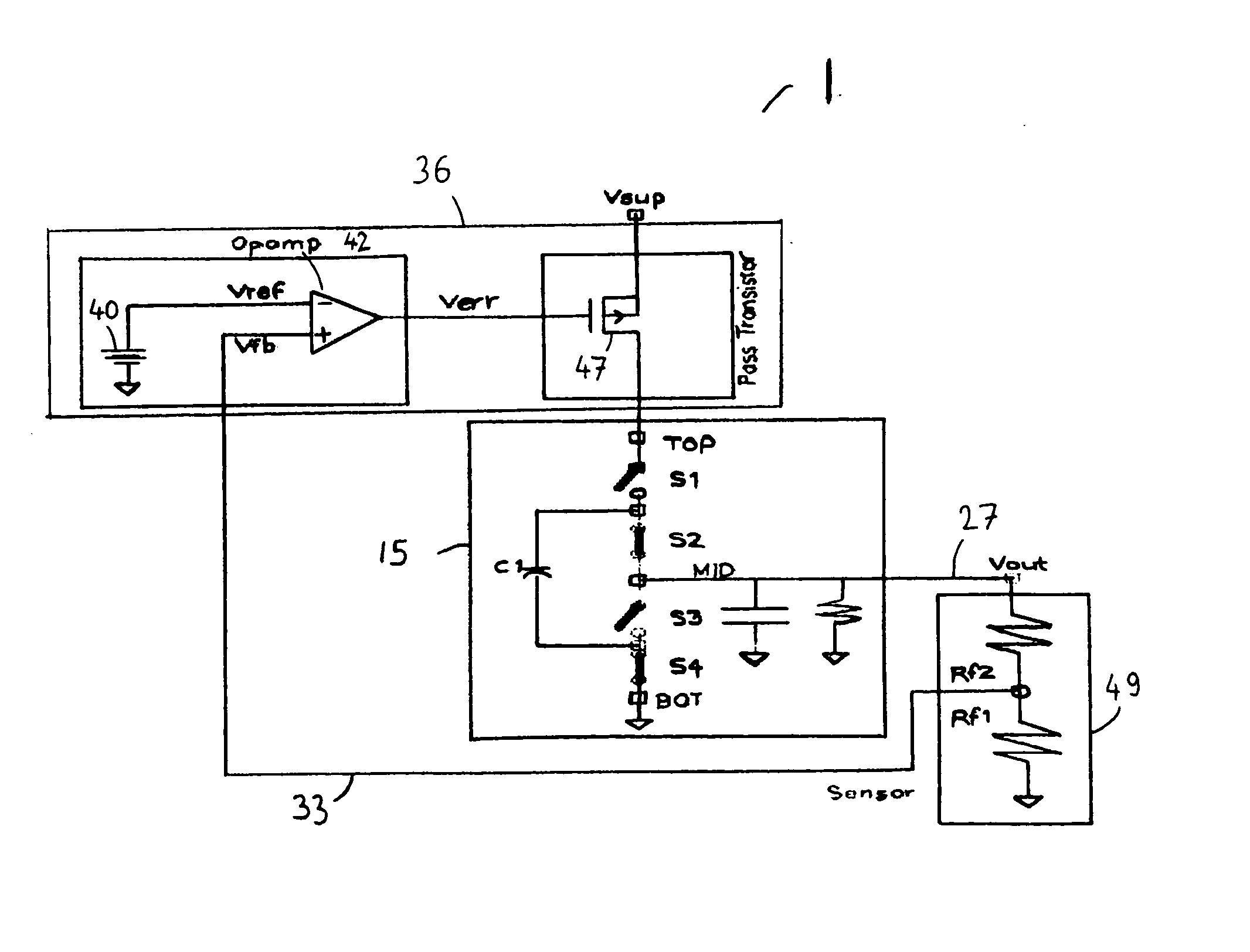
[0002] The present invention generally relates to power supplies, and more particularly, to switched capacitor charge pump power supplies for generating a regulated output voltage different from the supply voltage.

[0003] 2. Description of Related Art

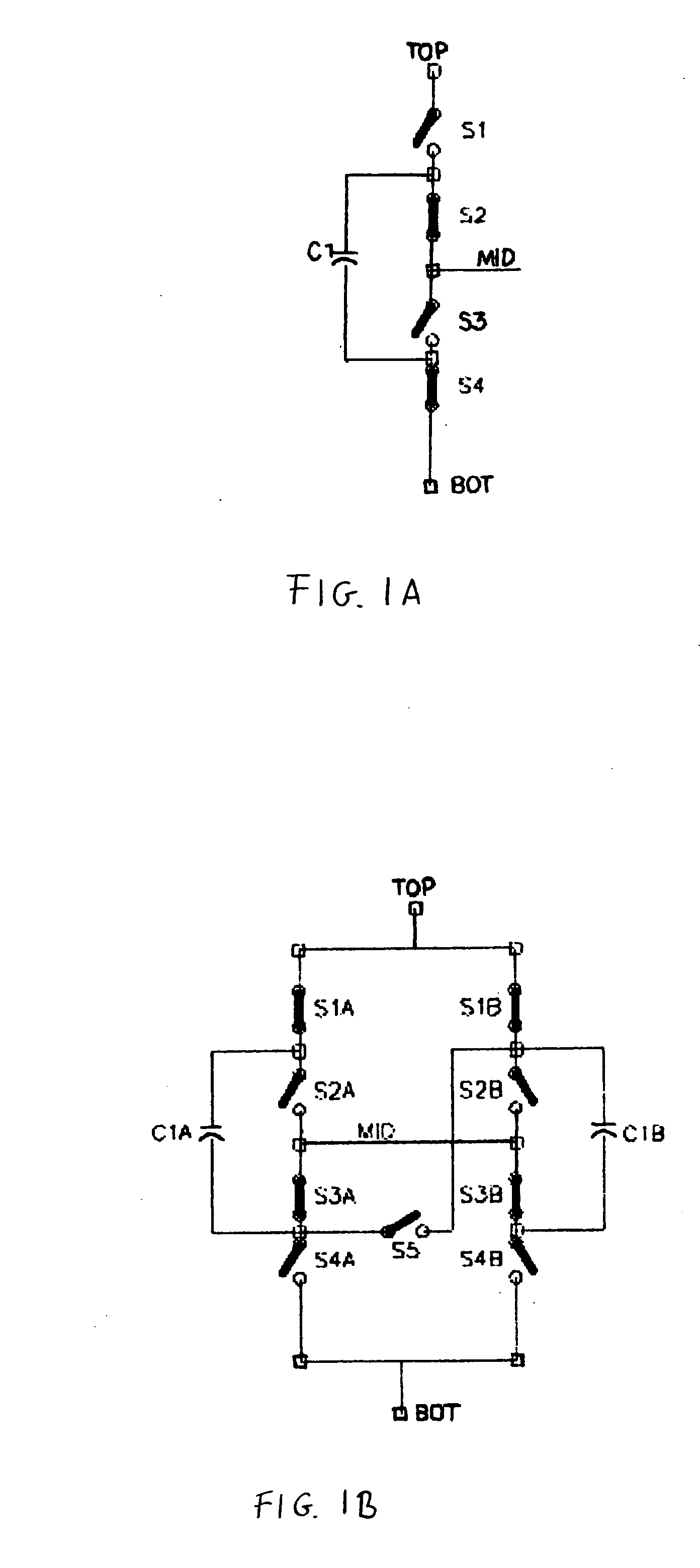
[0004] An unregulated switched capacitor DC / DC converter includes a switch array. FIG. 1A illustrates an existing converter topology. This converter utilizes one flying capacitor and four switches. FIG. 1B illustrates another existing topology with two flying capacitors and nine switches.

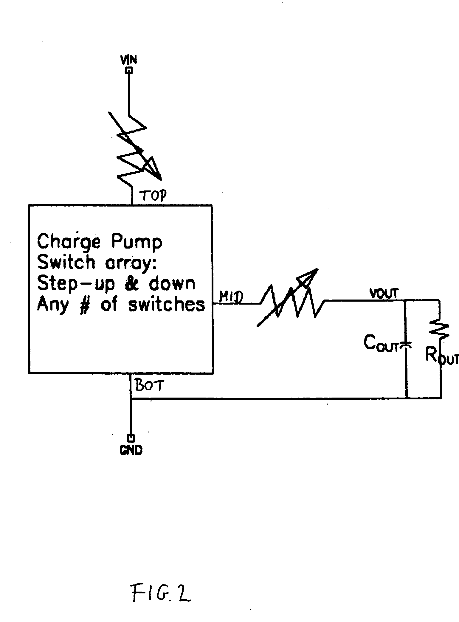
[0005] FIG. 2 illustrates a three terminal device that is equivalent to the switch array. By connecting the TOP, MID and BOT terminals with input, output, and ground in various combinations, step-up, step-down and inverter topologies are created.

[0006] FIG. 3 illustrates a 2:1 step-down charge pump. Two-phase non-overlapping clocks are used to drive the switches. In phase 1, the charging phase, switches S1 and S3...

Examples

Embodiment Construction

[0024] Embodiments of the present invention and their advantages are best understood by referring to FIGS. 1-8. Like numerals are used for like and corresponding parts of the various drawings.

[0025] The structure and operation of power control circuits will be described in relation to analog power control circuit 1 of FIG. 4. Then various power control circuits 2 will be described according to embodiments of the invention in relation to FIGS. 5-8.

[0026] In power control circuit 1, the regulation of output voltage V_out is achieved in an analog manner by coupling a V_DD supply voltage into voltage regulator block 36. In power control circuit 1 voltage regulator block 36 regulates the fraction of the V_DD supply voltage, which reaches switch array 15.

[0027] Voltage regulator block 36 includes reference voltage supply 40, providing a predefined reference voltage V_ref. In some embodiment the value of reference voltage V_ref can be in the range of about 0.5V to 20V. Voltage regulator...