Shielded bitline architecture for dynamic random access memory (dram) arrays

一种存储器阵列、存储器的技术,应用在静态存储器、数字存储器信息、信息存储等方向,能够解决耗费芯片晶粒面积、装置费用增加、总动态随机存取存储器数组面积增加等问题

Inactive Publication Date: 2007-03-21
PROMOS TECH INC
View PDF0 Cites 3 Cited by
  • Summary
  • Abstract
  • Description
  • Claims
  • Application Information

AI Technical Summary

Problems solved by technology

However, the layout of bitline twists consumes on-chip die area, typically about six bitline pitches, thereby resulting in an increase in the total DRAM array area required, with a concomitant increase in device cost
In addition, when the twisting of the bit lines ensures that the bit line to bit line coupling becomes a "common mode", the coupling still cannot be reduced

Method used


Image

  • Shielded bitline architecture for dynamic random access memory (dram) arrays
  • Shielded bitline architecture for dynamic random access memory (dram) arrays
  • Shielded bitline architecture for dynamic random access memory (dram) arrays

Examples


Embodiment Construction

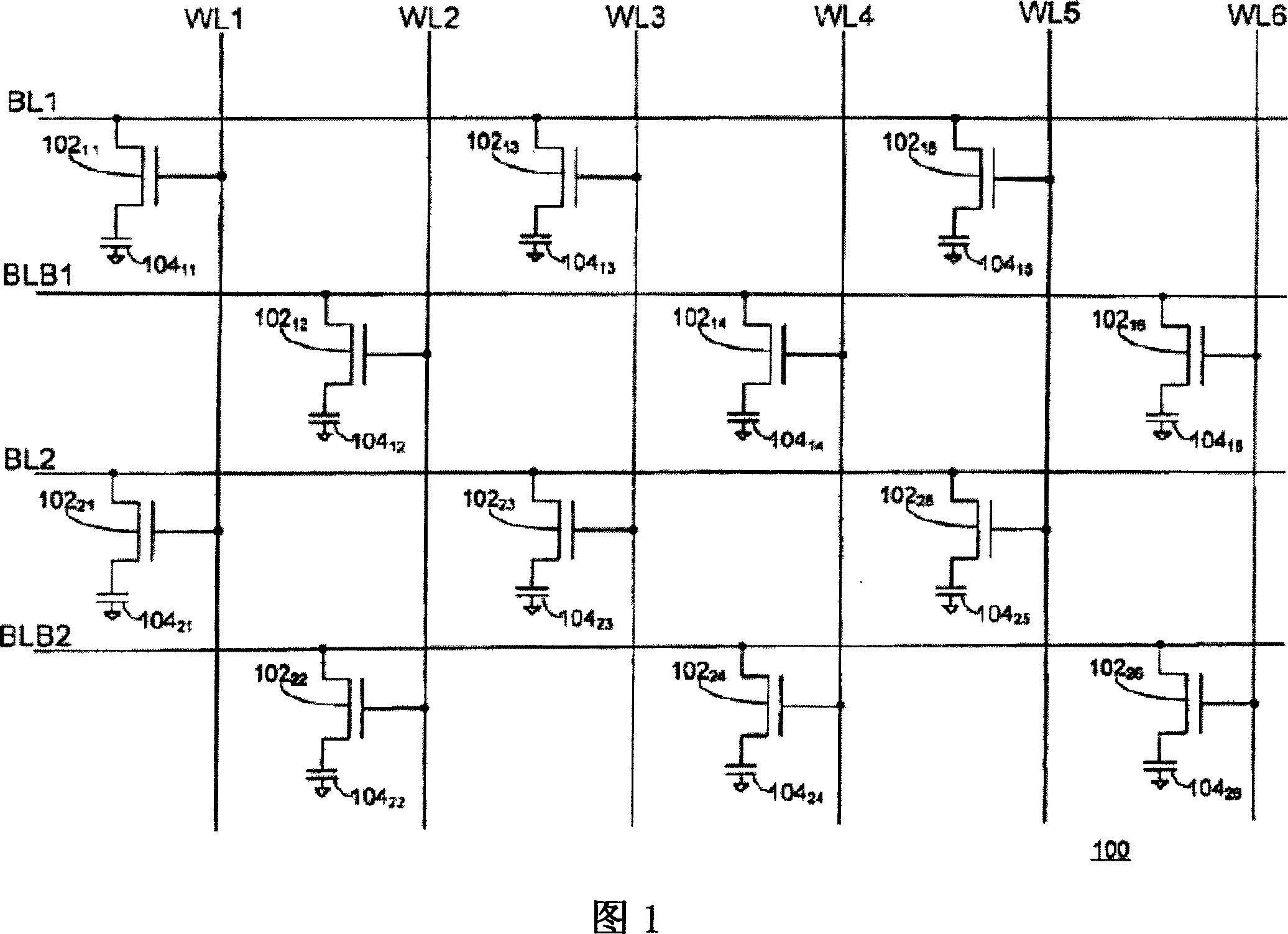
[0054] Referring to FIG. 1 , it is a part of a typical DRAM array 100 with a folded bit line structure, wherein the bit lines marked as BLB (bitline bar, such as BLB1 and BLB2) serve as the bit lines marked as BL (such as BL1 and BL2) Line reference, which is input to a sense amplifier (not shown) when the word line (WL) is "high".

[0055] Each memory cell of the DRAM array 100 includes an N-type channel access transistor 102 11 ~102 16 and 102 21 ~102 26 , and respectively include a connected storage capacitor 104 11 ~104 16 and 104 21 ~104 26 . The drain of each transistor 102 is coupled to one of the corresponding complementary bit lines, its gate is coupled to one of the word lines WL1-WL6, the source of each transistor 102 is coupled to the plate of the corresponding capacitor 104, the other plate of which Depending on the memory technology used, it is decided to couple to circuit ground (VSS) or to a common plate line.

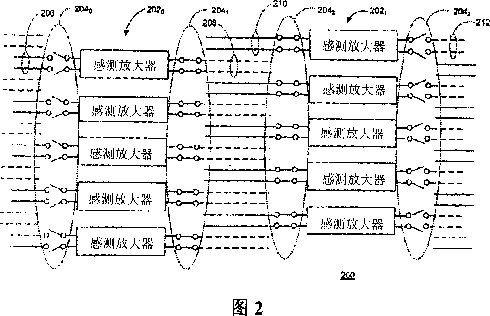
[0056] In the part of the dynamic random...


PUM


Abstract

A shielded bitline architecture for DRAM memories and integrated circuit devices incorporating embedded DRAM is disclosed herein which comprises a shared sense amplifier, folded bitline array using a bitline from an adjacent, non-active subarray as a reference for a bitline in an active array.

Description

technical field [0001] The present invention relates to the field of integrated circuit (IC) memory devices, including dynamic random access memory (DRAM) devices and other integrated circuit devices incorporating embedded dynamic random access memory. In particular, it relates to a shielded bit line structure for a dynamic random access memory array. Background technique [0002] There are a variety of DRAM base devices or integrated circuits with embedded memory arrays, including Extended Data Output (EDO) DRAM, Synchronous DRAM (SDRAM), Double Data Rate (DDR) DRAM Random Access Memory, DDR3 Dynamic Random Access Memory (DDR3 DRAM), and the like. Regardless of configuration, the main purpose of DRAM is to store data. The main function of the memory is that data can be written into the memory, read from it or updated periodically to maintain the integrity of the stored data. In today's high-density designs, each DRAM cell typically consists of a single access transistor ...

Claims


Application Information

Patent Timeline
Patent Type & Authority Applications(China)
IPC IPC(8): G11C11/4094
CPCG11C7/02G11C7/18G11C2207/104G11C11/4097
Inventor 道格拉斯·布莱恩·巴特勒
Owner PROMOS TECH INC
Why Eureka
Try Eureka