Electronic circuit design

a technology of electronic circuits and circuits, applied in the field of electronic circuit design, can solve the problems of large design instruction files, and increasing the storage requirements of the myriad of design feature instructions and design instruction files, so as to reduce the size of design data, reduce data storage and computer resource requirements, and leverage the effect of features redundancy

Inactive Publication Date: 2006-05-16
IBM CORP
View PDF7 Cites 5 Cited by
  • Summary
  • Abstract
  • Description
  • Claims
  • Application Information

AI Technical Summary

Benefits of technology

[0012]The invention includes a method, system, program product and database for electronic circuit design configured to reduce data storage and computer resource requirements. The invention is binary based and leverages the redundancy of features in most electronic circuit designs by using templates of unique design features. Each template includes an offset instruction for positioning the unique design feature relative to a control point rather than a previous feature. The control point is positioned within a design grid according to data in a template recall that replaces the unique design feature's instruction set in an instruction list of a design instruction file. Because each template is stored once, and only once, considerable reduction in design data size is achieved. In addition, each template recall has a fixed width data format that restrains data size and allows more efficient processing.

Problems solved by technology

Although automated design systems provide substantial support to designers, the ever-increasing complexity of circuits has resulted in design instruction files of extremely large proportions.
The large design instruction files strain resources in a number of ways.
Second, storage requirements of the myriad of design feature instructions and the design instruction files must continuously be increased.
As a result, the expense of design workstations and related storage facilities has become an increasing problem.
Unfortunately, each time a feature is required in a design, its respective instruction portion is repeated in the instruction list.
This redundant usage of instruction portions occurs despite the fact that most designers create designs that have a fairly low number of unique features.
First, compartmentalizing the instruction list and removing data from the list are slow.
Another problem with the conventional design instruction file is created by the fact that each feature may have its own peculiarities requiring less or more data.
This causes, a standard processor that is based on 4 byte or 8 byte multiples, e.g., a 32 bit or a 64 bit processor, to process data inefficiently.
Unfortunately, this format suffers from a number of drawbacks in use as a design system.
First, it is ASCII based, which greatly increases data instruction file size.
Second, instruction lists are limited to shape characteristics only.
As a result, the Gerber format is not appropriate for design database use.
For example, a semiconductor design of a 60-sided polygon may require a feature to be created, for example, 1531 separate times. The GL1 language has all of the features stored as variable width data objects, which is inefficient because either a look up table of memory locations for features must be created and maintained, or serial reading of the entire feature list need be undertaken to access a given feature.

Method used


Image

  • Electronic circuit design
  • Electronic circuit design
  • Electronic circuit design

Examples


Embodiment Construction

[0027]For purposes of convenience only, the following description includes the following headings: I. System Overview, II. Template, III. Design Instruction File, IV. Attribute Look Up Lists, and V. Operation Methodology.

I. System Overview

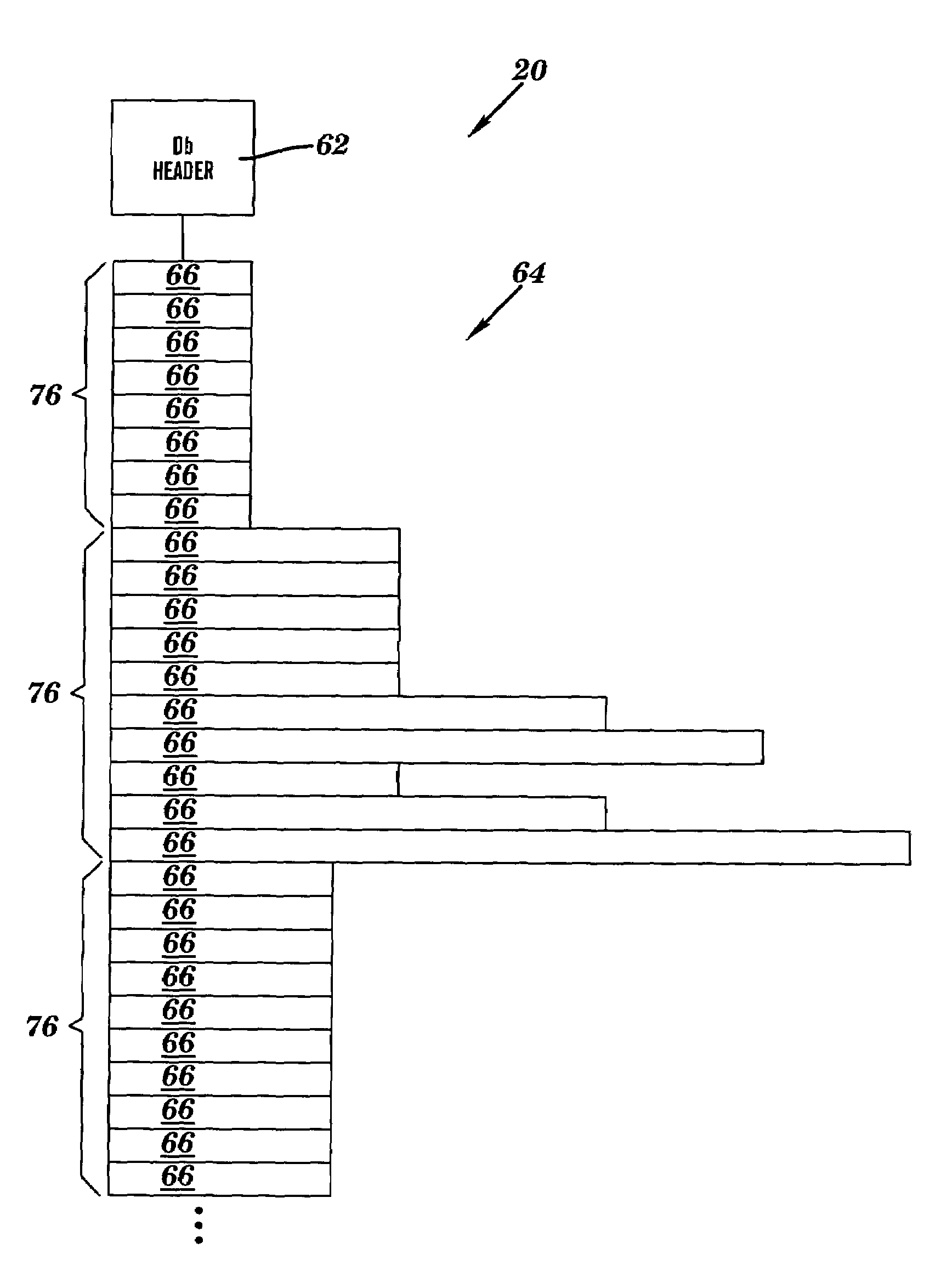
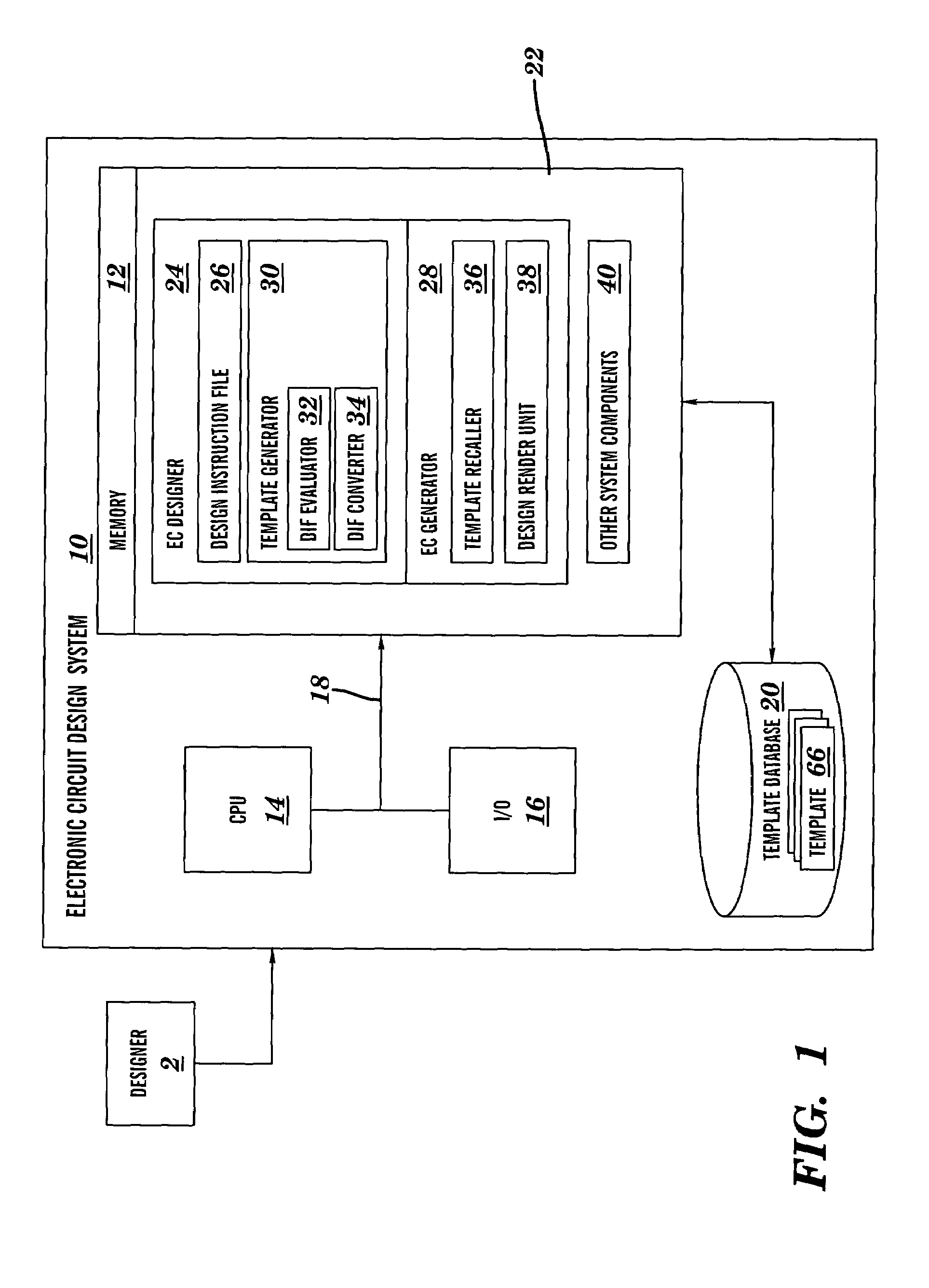
[0028]With reference to the accompanying drawings, FIG. 1 is a block diagram of an electronic circuit design system 10 in accordance with the invention. System 10 includes a memory 12, a central processing unit (CPU)14, input / output devices (I / O) 16 and a bus 18. A template database 20 is also provided for storage of feature templates and other data relative to processing tasks, as will be described in greater detail below. Memory 12 includes a program product 22 that, when executed by CPU 14, comprises various functional capabilities described in further detail below. Memory 12 (and database 20) may comprise any known type of data storage system and / or transmission media, including magnetic media, optical media, random access memory (RAM), read on...


PUM


Abstract

A method, system, program product and database for electronic circuit design configured to reduce data storage and computer resource requirements. The invention is binary based and leverages the redundancy of features in most electronic circuit designs by using templates of unique design features. Each template includes offset instructions for positioning the unique design feature relative to a control point rather than a previous feature. The control point is positioned within a design grid according to data in a template recall that replaces the unique design feature's instruction set in an instruction list of a design instruction file. Because each template is stored once, and only once, considerable reduction in design data size is achieved. In addition, each template recall has a fixed width data format that restrains data size and allows more efficient processing.

Description

BACKGROUND OF THE INVENTION[0001]1. Technical Field[0002]The present invention relates generally to electronic circuit design, and more particularly to a system, method, program product and database for electronic circuit design.[0003]2. Related Art[0004]Electronic circuits are often designed using automated design systems to increase the speed of the design process, and to allow evaluation of a design prior to actual production. In a conventional setting, a designer uses the automated design system to generate a circuit by inputting data at a computer workstation. A designer will typically design a circuit in terms of functional aspects and then deconstruct each aspect into ever-smaller features. For example, a designer may establish a functional aspect and then draw several simple features in laying out components for the functional aspect, and may free-hand a number of larger more unique features to handle special circumstances. Layout of features providing the functional aspects...

Claims


Application Information

Patent Timeline
Patent Type & Authority Patents(United States)
IPC IPC(8): G06F17/50
CPCG06F17/50G06F30/00
Inventor MOYER, THOMAS P.
Owner IBM CORP
Why Eureka
Try Eureka