Method of forming thick-film wiring and method of producing laminated electronic component

a technology of thick-film wiring and laminated electronic components, which is applied in the direction of dielectric characteristics, coupling device connections, conductive pattern formation, etc., can solve the problems of long processing time and difficult formation of conventional thick-film wirings

Inactive Publication Date: 2006-05-23
MURATA MFG CO LTD
View PDF12 Cites 9 Cited by
  • Summary
  • Abstract
  • Description
  • Claims
  • Application Information

AI Technical Summary

Benefits of technology

[0011]To overcome the problems described above, preferred embodiments of the present invention provide a method of forming a thick-film wiring in which an electroconductive paste can be securely transferred from an intaglio plate onto a substrate, even if the electroconductive paste is thicker than a predetermined thickness.

Problems solved by technology

However, according to this method, it is necessary to repeat the filling of the electroconductive paste and the drying several times. Thus, because the number of processing steps is large, the processing time is long.
Thus, conventional thick-film wirings are formed with much difficulty.

Method used


Image

  • Method of forming thick-film wiring and method of producing laminated electronic component
  • Method of forming thick-film wiring and method of producing laminated electronic component
  • Method of forming thick-film wiring and method of producing laminated electronic component

Examples


example 1

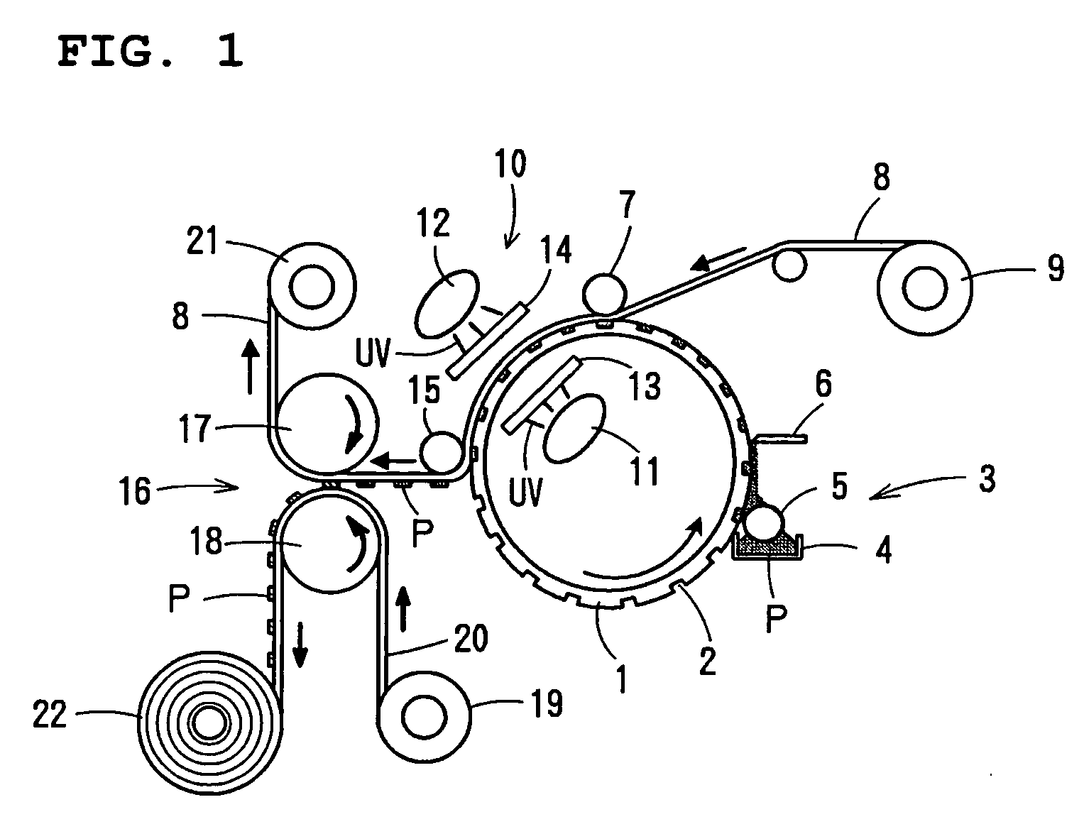
[0057]FIG. 1 illustrates a first transfer apparatus which carries out methods according to preferred embodiments of the present invention.

[0058]The transfer apparatus is provided with an intaglio plate 1 having a substantially cylindrical drum shape. The intaglio plate 1 is preferably made of a material having a UV transmittance such as transparent glass. A pattern groove 2 corresponding to a desired thick-film wiring pattern is formed on the outer surface of the intaglio plate 1. Preferably, the depth of the pattern groove 2 is at least about 20 μm, and the aspect ratio (longitudinal length / transverse length) is approximately 1. Preferably, the diameter of the intaglio plate 1 is in the range of about 300 mm to about 600 mm. The intaglio plate 1 is rotated at a constant speed in the direction shown by an arrow in FIG. 1.

[0059]A feeding unit 3 for supplying the electroconductive paste P to the pattern groove 2 is provided on the periphery of the intaglio plate 1. The electroconducti...

example 2

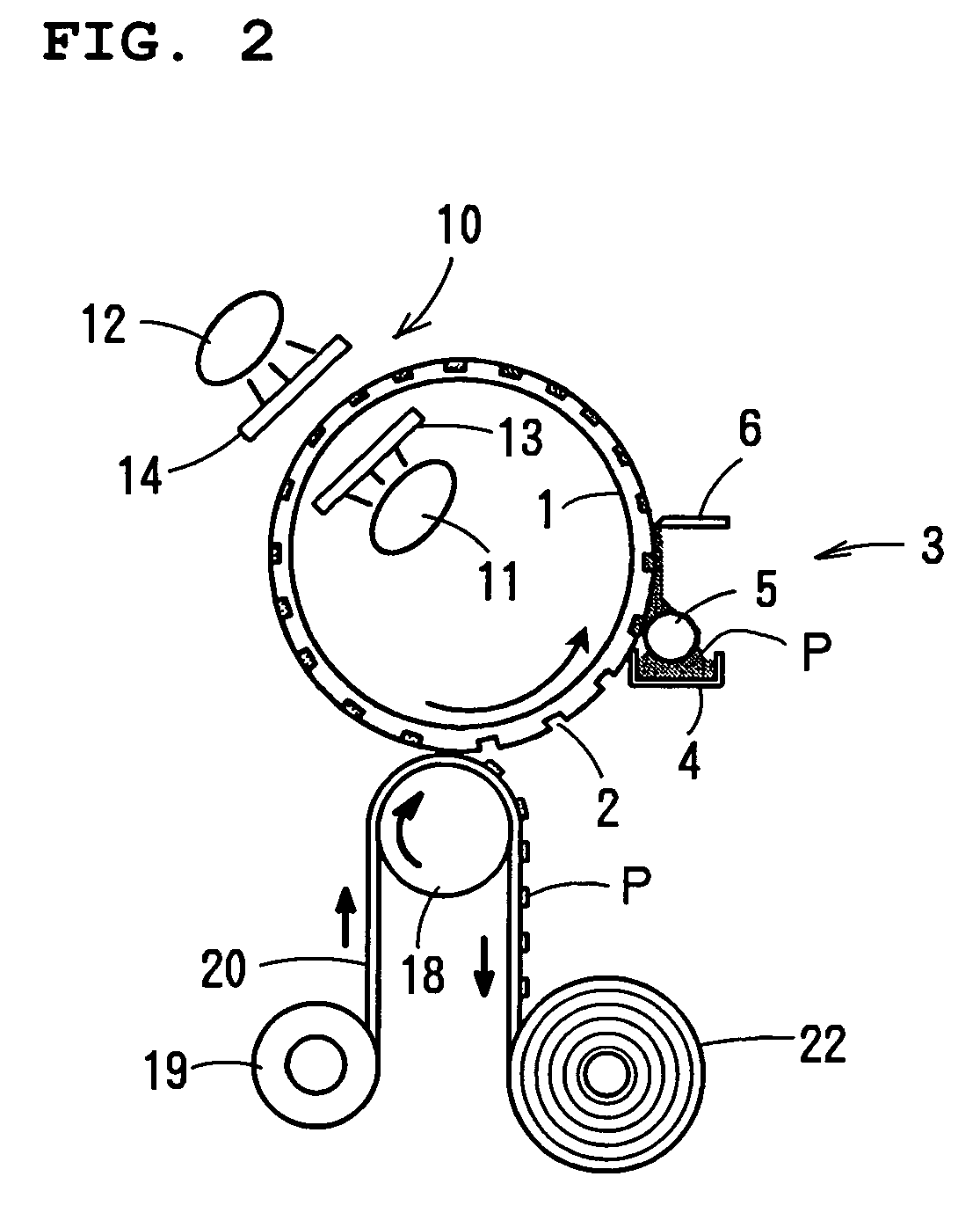
[0073]FIG. 2 illustrates a second transfer apparatus which carries out a method according to preferred embodiments of the present invention.

[0074]In this Example, the electroconductive paste P is transferred directly from the intaglio plate 1 to the substrate 20, not using the carrier sheet 8 as an intermediate piece. The components of Example 2 which are the same as or equivalent to those of the Example 1 are designated by the same reference numerals, and the description is not repeated.

[0075]The electroconductive paste P is filled into the pattern groove 2 by the feeding unit 3. The electroconductive paste P is irradiated by UV rays from the light source 11 and 12 arranged on the front and back sides (inner and outer sides) of the intaglio plate 1. When UV rays are irradiated from the front and back sides of the intaglio plate 1, a part of the electroconductive paste P exposed on the surface of the intaglio plate 1 is directly irradiated by the UV rays. A part of the electroconduc...

example 3

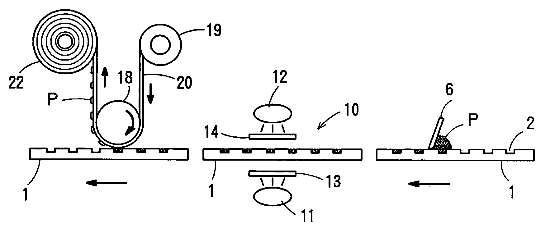
[0077]FIG. 3 illustrates a third transfer unit which carries out a method according to preferred embodiments of the present invention.

[0078]In this example, the electroconductive paste P is transferred directly to the substrate 20 not using the intermediate piece. Moreover, as the substrate 20, a hard substrate such as a fired ceramic plate is used.

[0079]The electroconductive paste P filled in the pattern groove 2 and hardened to have a predetermined hardness by UV lamps 11 and 12, which are arranged on the front and back sides (from the inner and outer sides) of the intaglio plate 1, is directly transferred to the substrate 20 which is being moved horizontally in contact with the lower end surface of the intaglio plate 1.

[0080]In this case, the entire periphery of the electroconductive paste P filled in the pattern groove 2 is hardened (dried). Thus, the cohesive force of the electroconductive paste P is increased, and the transferring-property of the paste to be transferred to the...


PUM

PropertyMeasurementUnit
thicknessaaaaaaaaaa
thicknessaaaaaaaaaa
depthaaaaaaaaaa

Abstract

In a method of forming a thick-film wiring on a substrate, photosensitive-electroconductive paste is filled into a pattern groove formed on the surface of a light-transmitting intaglio plate. The pattern groove corresponds to a desired thick-film wiring pattern. The photosensitive-electroconductive paste filled in the pattern groove are irradiated with light-rays from the front and back sides of the intaglio plate to cause the paste to harden until the overall peripheral surface of the electroconductive paste has a predetermined hardness. The electroconductive paste hardened in the pattern grooves of the intaglio plate is transferred to an intermediate piece. Then, the electroconductive paste is transferred from the intermediate piece to a substrate. Thereafter, the electroconductive paste is fired, whereby a thick-film wiring is formed on the substrate.

Description

BACKGROUND OF THE INVENTION[0001]1. Field of the Invention[0002]The present invention relates to a method of forming a thick-film wiring, and more particularly, to a method of forming on a substrate a thick-film wiring having a fine line-width and a relatively large film-thickness, e.g., at least about 10 μm.[0003]2. Description of the Related Art[0004]In recent years, with the sizes of electronic devices being reduced, the reduction in size of electronic components used in the electronic devices has been required. In these situations, thick-film wirings are needed because the wiring pattern is fine and the line resistances of the wiring pattern are reduced.[0005]To satisfy the above-described requirements, as proposed in Japanese Patent No. 3039265, electroconductive paste is filled in the engraved portions of an intaglio plate made of a flexible resin. The paste is dried. Then, additional electroconductive paste is added to the engraved portions of the flexible resin intaglio plat...

Claims


Application Information

Patent Timeline
Patent Type & Authority Patents(United States)
IPC IPC(8): H01L21/44B41M1/10H01R13/10B41F9/01H01L21/48H05K1/09H05K3/12H05K3/20
CPCH01L21/4857H01L21/4867H05K3/207H05K1/092H05K3/1275H05K2203/0534H05K2201/0108H05K2203/0113H05K2203/0143H05K3/20
Inventor ODA, TETSUYAFUJII, CHOICHIRONISHIKAWA, ETSUO
Owner MURATA MFG CO LTD
Why Eureka
Try Eureka