Semiconductor device having stiffener

a technology of semiconductor elements and stiffeners, which is applied in the direction of printed circuit aspects, sustainable manufacturing/processing, final product manufacturing, etc., can solve the problems of further reducing etc., to minimize the warp of the substrate and the warp of the semiconductor element.

Active Publication Date: 2006-05-30
FUJITSU LTD
View PDF19 Cites 10 Cited by
  • Summary
  • Abstract
  • Description
  • Claims
  • Application Information

AI Technical Summary

Benefits of technology

[0006]An object of the present invention is to provide a semiconductor device capable of further reducing the warp of the substrate and that of the semiconductor element.
[0010]As a result, the inventors of the present invention have studied the warp of the substrate and the warp of the semiconductor element in the semiconductor device provided with the stiffener, and it has been found that the warp of the substrate and the warp of the semiconductor element can be avoided by suitably selecting not only the characteristics of the stiffener but also the characteristics of the adhesive used for fixing the stiffener to the substrate. Accordingly, it is possible to further minimize the warp of the substrate and the warp of the semiconductor element if the characteristics of the material forming the respective members are properly selected to satisfy the above-mentioned relationship of between the coefficient of thermal expansion of the substrate and that of the stiffener and that of the adhesive, and the modulus of longitudinal elasticity of the adhesive.
[0011]Also, in the case of the semiconductor device having external terminals provided on the substrate around the stiffener, if a height of the stiffener is less than that of the external terminals, the external terminals formed as solder balls are assuredly bonded to the terminals of the printed circuit board and the stiffener is brought into contact with the surface of the printed circuit board, whereby the stiffener exhibits a stand-off function to properly connect the substrate to the printed circuit board. Thus, the warp of the substrate and the warp of the semiconductor element is further minimized.

Problems solved by technology

In a semiconductor device having a semiconductor element mounted on a substrate, a problem arises in that a warp may occur in the substrate and in the semiconductor element as a result of a difference between the coefficient of thermal expansion of the semiconductor element and that of the substrate.
However, because the warp of the substrate and that of the semiconductor element are not completely eliminated, there is still a requirement for further reducing the warp of the substrate and of the semiconductor element.

Method used


Image

  • Semiconductor device having stiffener
  • Semiconductor device having stiffener
  • Semiconductor device having stiffener

Examples


Embodiment Construction

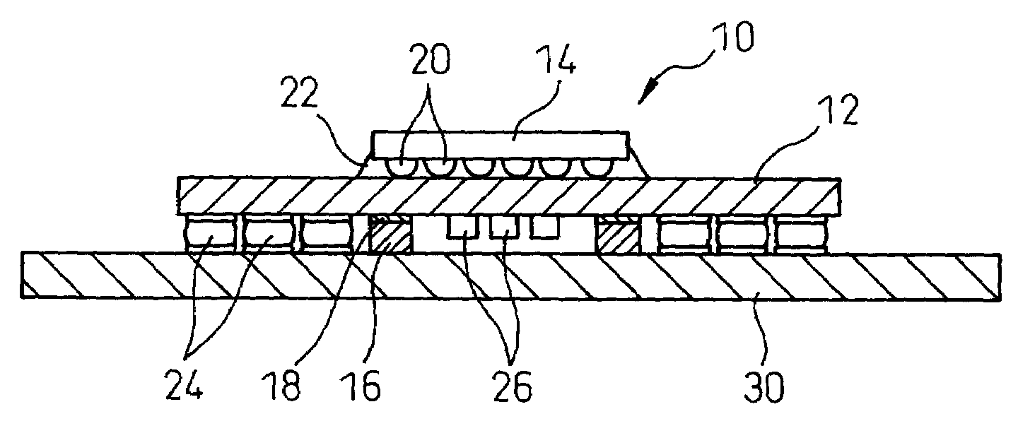
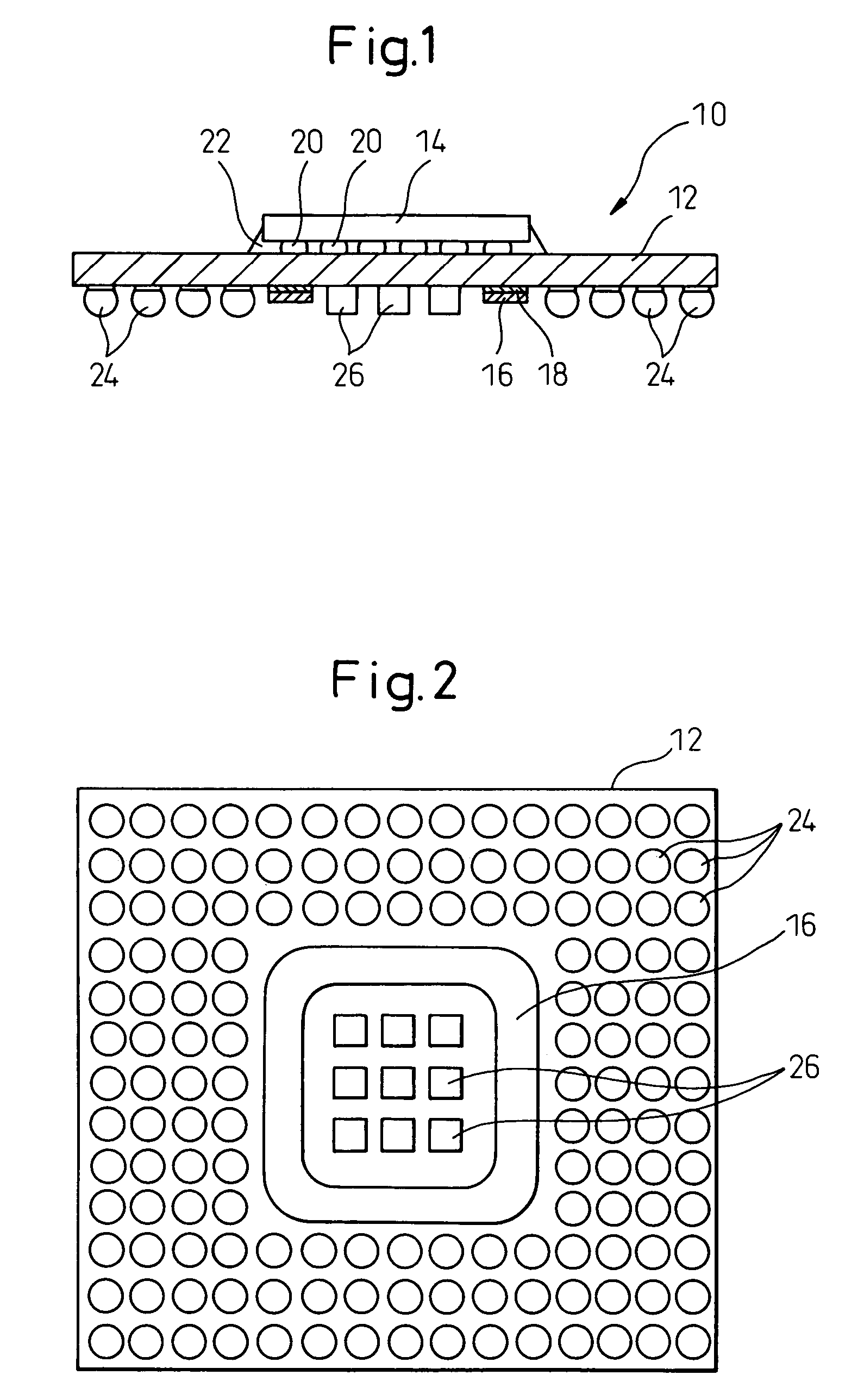
[0021]The preferred embodiments of the present invention will now be described with reference to the attached drawings. FIG. 1 is a cross-sectional view of the semiconductor device according to the present invention and FIG. 2 is a bottom view of the semiconductor device shown in FIG. 1. In FIGS. 1 and 2, the semiconductor device 10 includes a substrate 12, a semiconductor element (an LSI chip) 14 mounted on the substrate 12, and a stiffener 16 attached via an adhesive 18 to a surface of the substrate 12 opposite that carrying the semiconductor element 14 thereon. Bumps (solder balls) 20 are provided on electrode pads of the semiconductor element 14, and joined to corresponding electrode pads of the substrate 12 by flip-chip bonding. An under-fill material 22 is filled around the bumps 20 in a gap between the semiconductor element 14 and the substrate 12.

[0022]The stiffener 16 is a frame-like member having an outer contour generally identical to that of the semiconductor element. Th...


PUM


Abstract

A semiconductor device including a substrate, a semiconductor element mounted on the substrate and a stiffener attached via an adhesive to a surface of the substrate opposite a surface thereof on which the semiconductor element is mounted. The adhesive has a coefficient of thermal expansion smaller than that of the substrate and that of the stiffener, and the modulus of longitudinal elasticity of the adhesive is equal to or larger than 10 GPa. Otherwise, the adhesive has a coefficient of thermal expansion larger than that of the substrate and that of the stiffener, and the modulus of longitudinal elasticity of the adhesive is equal to or smaller than 10 GPa. The height of the stiffener is less than that of the external terminals.

Description

BACKGROUND OF THE INVENTION[0001]1. Field of the Invention[0002]The present invention relates to a semiconductor device provided with a stiffener.[0003]2. Description of the Related Art[0004]In a semiconductor device having a semiconductor element mounted on a substrate, a problem arises in that a warp may occur in the substrate and in the semiconductor element as a result of a difference between the coefficient of thermal expansion of the semiconductor element and that of the substrate. Accordingly, there have been proposals wherein a stiffener (a reinforcement member) is attached to the surface of the substrate opposite to that mounting the semiconductor element thereon to prevent the substrate and the semiconductor element from warping (for example, see Japanese Unexamined Patent Publication No. 3-295263, No. 6-204656, Japanese Unexamined Patent Publication No. 6-4579, No. 8-153938, No. 6-82839, No. 11-260953, No. 2000-174176, No. 2001-101375, No. 2001-15561, No. 2002-231769, and...

Claims


Application Information

Patent Timeline
Patent Type & Authority Patents(United States)
IPC IPC(8): H01L23/48H01L23/52
CPCH01L23/562H05K3/303H01L23/3128H05K3/305H05K2201/10568H05K2201/10734H05K2201/2036H01L2224/73204H01L2224/32225H01L2224/16225H01L2924/00H01L2924/00014H01L2924/00011Y02P70/50H01L23/16H01L2224/0401
Inventor KANDA, TAKASHIFUKUZONO, KENJI
Owner FUJITSU LTD
Why Eureka
Try Eureka