Method, apparatus and magnet assembly for enhancing and localizing a capacitively coupled plasma

a capacitively coupled plasma and magnet assembly technology, applied in the direction of coatings, chemical vapor deposition coatings, electric discharge tubes, etc., can solve the problems of arcing within the chamber, damage devices in integrated circuits, high and often excessive rf voltages, etc., and achieve the effect of avoiding wafer damag

Inactive Publication Date: 2006-06-13
TOKYO ELECTRON LTD
View PDF27 Cites 34 Cited by
  • Summary
  • Abstract
  • Description
  • Claims
  • Application Information

AI Technical Summary

Benefits of technology

[0009]An objective of the present invention is to provide for the uniform distribution of a low voltage plasma across the surface of a substrate during processing, particularly in vacuum plasma processes for the manufacture of semiconductor wafers. A more particular objective of the invention is to provide a method, plasma source and processing apparatus for distributing a low-voltage high-density plasma at the surface of a wafer being processed that produces minimal charge distribution non-uniformity across the wafer and avoids wafer damage.

Problems solved by technology

This arrangement requires high and often excessive RF voltages to generate sufficient plasma density to perform the process efficiently.
Such high voltages can damage devices in integrated circuits as well as cause arcing within the chamber.
Further, with such systems, plasma uniformity and subsequently etch or deposition uniformity on the substrate are unpredictable and often unsatisfactory.
Further, using a delicate substrate exclusively as an electrode usually results in excessive substrate temperature.
If the magnetic field forms a closed loop, the electrons have no fixed point of exit from the field and are trapped, potentially indefinitely, under the magnetic field.
This trapping of electrons near the electrode surface results in larger amounts of energy being delivered to the electrons per volt of RF sheath potential.
A major drawback of magnetic enhancement in the prior art plasma processing of integrated circuits is device damage due to non-uniform charging effects of the substrate.
A non-uniform charge distribution along an insulated substrate surface results in voltage gradients across devices on the substrate, which can lead to voltage breakdown.
Non-uniform charging of the substrate can be caused by strongly non-uniform plasma density across the substrate surface.
Such non-uniformity in plasma can be caused by lines of magnetic flux intersecting the substrate surface at predominantly normal angles of incidence at different strengths across the surface of the substrate or in regions where the ionizing electrons are being produced.
A main drawback of this scheme is the need for costly and complex rotating hardware.

Method used


Image

  • Method, apparatus and magnet assembly for enhancing and localizing a capacitively coupled plasma
  • Method, apparatus and magnet assembly for enhancing and localizing a capacitively coupled plasma
  • Method, apparatus and magnet assembly for enhancing and localizing a capacitively coupled plasma

Examples


Embodiment Construction

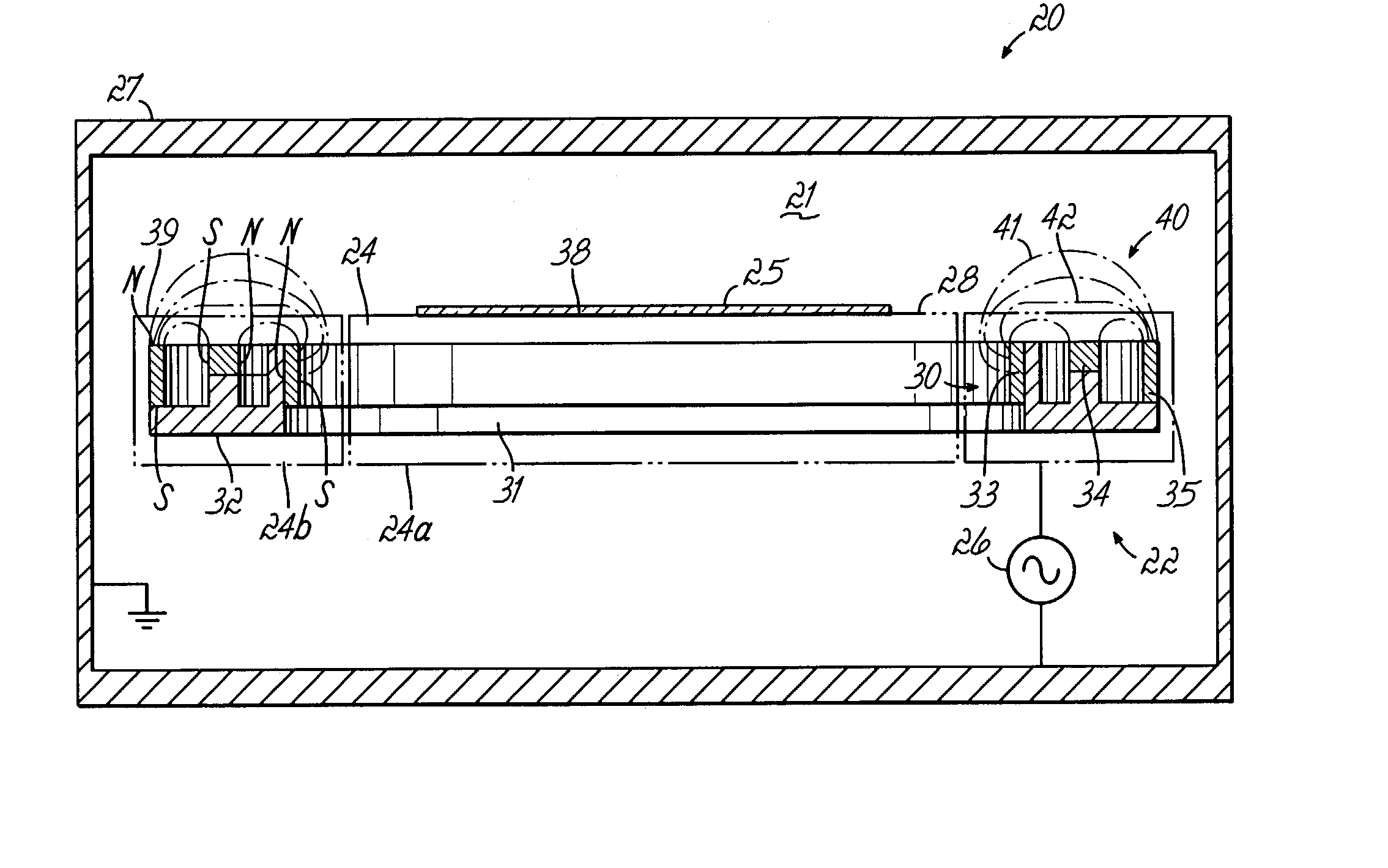
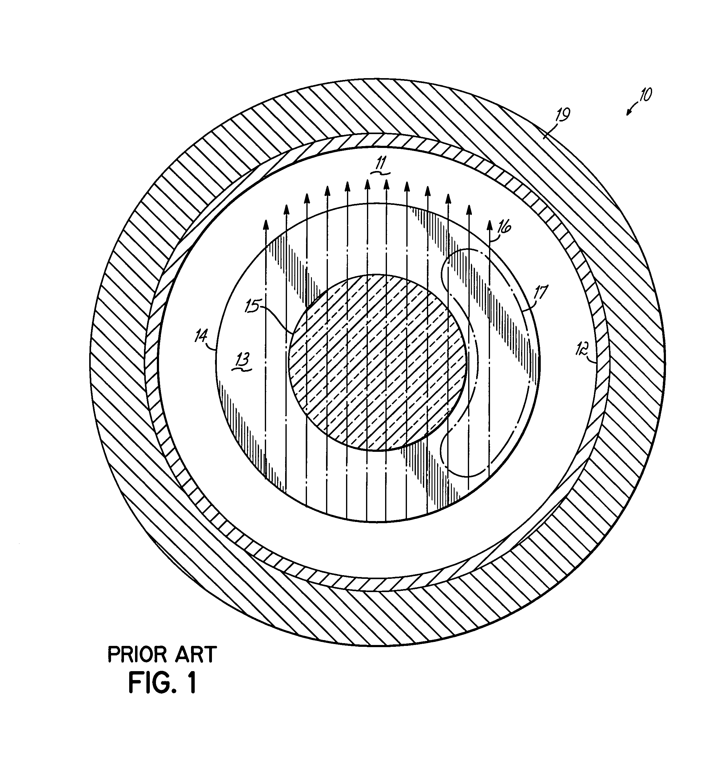
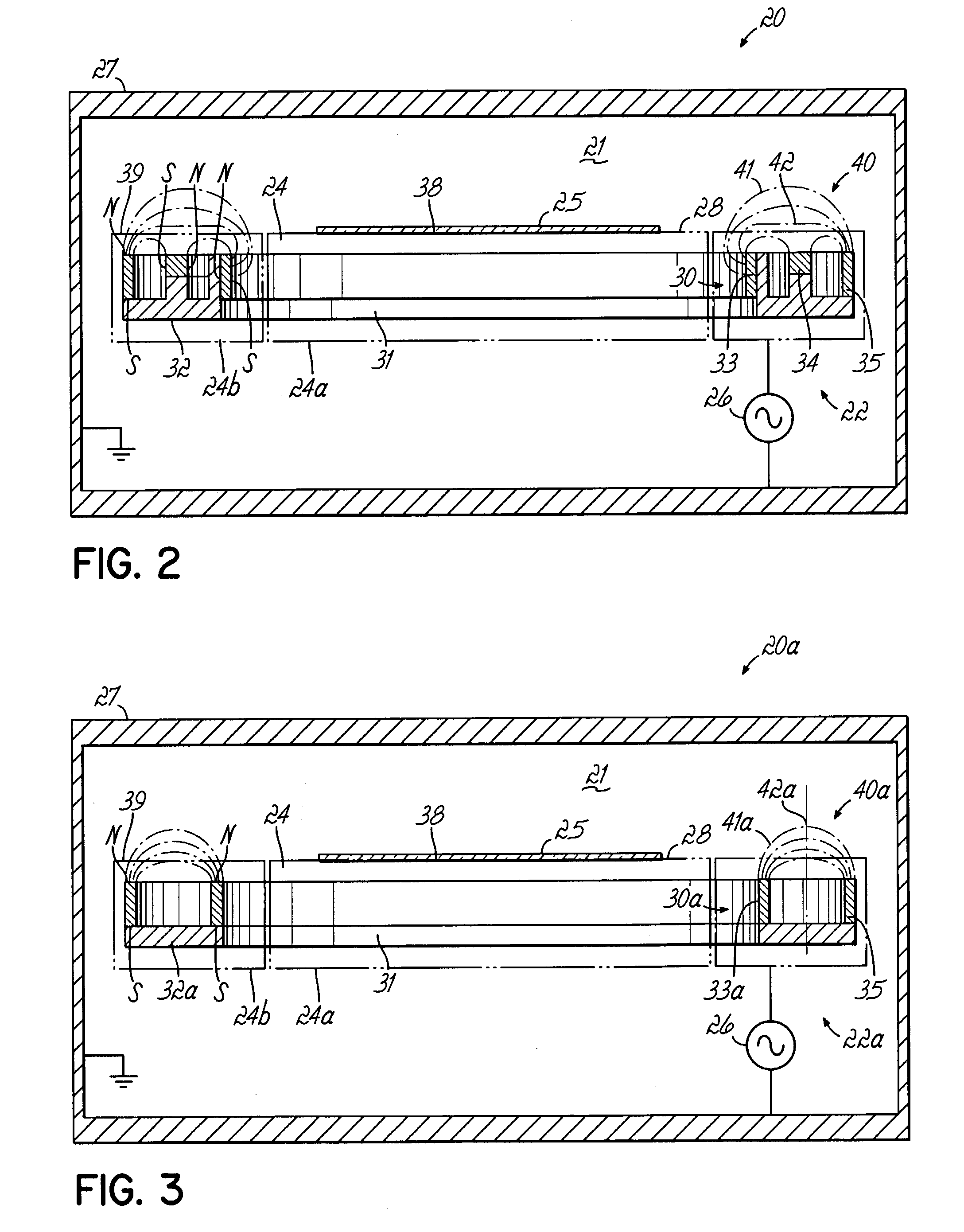
[0023]In the prior art plasma processing apparatus 10 of FIG. 1, a plasma processing chamber 11 is illustrated in cross-section through chamber wall 12 and facing a substrate supporting surface 13 of a substrate support 14 on which is centrally mounted a semiconductor wafer 15 for processing. Magnet structure (not shown), which may be outside of the chamber 11, generates a magnetic field 16 that is generally parallel to the substrate support surface 13. An RF generator (also not shown) coupled to the support 14, capacitively couples RF energy into gas within the chamber 11 to energize a plasma. The plasma tends to be produced in a cycloid region 17 where cycloid orbits of electrons are induced by the RF energy in the presence of the magnetic field 16. The plasma is axially unsymmetrical and otherwise non-uniform. In such an apparatus 10, the plasma is frequently made axially symmetrical at least by the use of a magnet arrangement that is made to rotate by costly and complex rotation...


PUM

PropertyMeasurementUnit
magnetic fieldaaaaaaaaaa
magnetic polesaaaaaaaaaa
polar axisaaaaaaaaaa

Abstract

A magnetically enhanced plasma is produced with a permanent magnet assembly adjacent to a radio frequency (RF) biased wafer support electrode in a vacuum processing chamber of a semiconductor wafer processing apparatus. An annular peripheral region is provided on the wafer support around the perimeter of the wafer being processed. A magnet arrangement using a plurality of magnet rings forms a magnetic tunnel over the peripheral region at which the plasma is generated away from the wafer. The magnetic field has components parallel to the substrate support surface over the annular peripheral region but which are perpendicular to the surface at the wafer. Preferably, the magnetic field has a flat portion parallel to the support surface in the peripheral region. Plasma propagates by diffusion from the peripheral region across the wafer surface. The magnets can be manipulated to optimize plasma uniformity adjacent the substrate being processed.

Description

[0001]This invention relates to the plasma processing of substrates, particularly semiconductor wafer substrates, and to the generation, enhancement and control of plasmas, particularly capacitively coupled plasmas, in such processing.BACKGROUND OF THE INVENTION[0002]Plasma is used in the production of semiconductors in processes such as plasma etching, ionized physical vapor deposition (iPVD) and plasma-enhanced chemical vapor deposition (PECVD). Plasma is often produced for such applications by capacitively coupling energy into a processing gas in a vacuum chamber to dissociate molecules of the gas into reactive free radicals and atoms, to excite molecules, radicals and ions of the gas into higher electronic states, to ionize molecules and atoms of reactive and inert gas, and to accelerate ions into trajectories normal to the surface of a substrate and onto the substrate.[0003]In PECVD plasma processing applications, capacitive coupling may be used to dissociate and excite molecul...

Claims


Application Information

Patent Timeline
Patent Type & Authority Patents(United States)
IPC IPC(8): H01L21/302C23C16/509H01J37/32
CPCC23C16/509H01J37/3266H01J37/32623H01J37/32091H01L21/302H01L21/461
Inventor RUSSELL, DERREK ANDREW
Owner TOKYO ELECTRON LTD
Why Eureka
Try Eureka