Method of manufacturing an optical element using a hologram

a manufacturing method and optical element technology, applied in the field of optical element manufacturing, can solve the problems of reducing the final accuracy of testing the optical surface, the inability of the hologram to allow the interferometer set, etc., and achieve the effect of uniform line density of the hologram

Inactive Publication Date: 2006-06-13
CARL ZEISS SMT GMBH
View PDF22 Cites 31 Cited by
  • Summary
  • Abstract
  • Description
  • Claims
  • Application Information

AI Technical Summary

Benefits of technology

[0023]Exemplary embodiments to all of the above mentioned aspects comprise disposing refractive elements in the beam path, upstream or downstream of the hologram. Such a refractive element may contribute to the generation of the wavefronts in

Problems solved by technology

Thus, the hologram will not allow an interferometer set up in which the beam of measuring light traversing the hologram has an overal

Method used


Image

  • Method of manufacturing an optical element using a hologram
  • Method of manufacturing an optical element using a hologram
  • Method of manufacturing an optical element using a hologram

Examples


Embodiment Construction

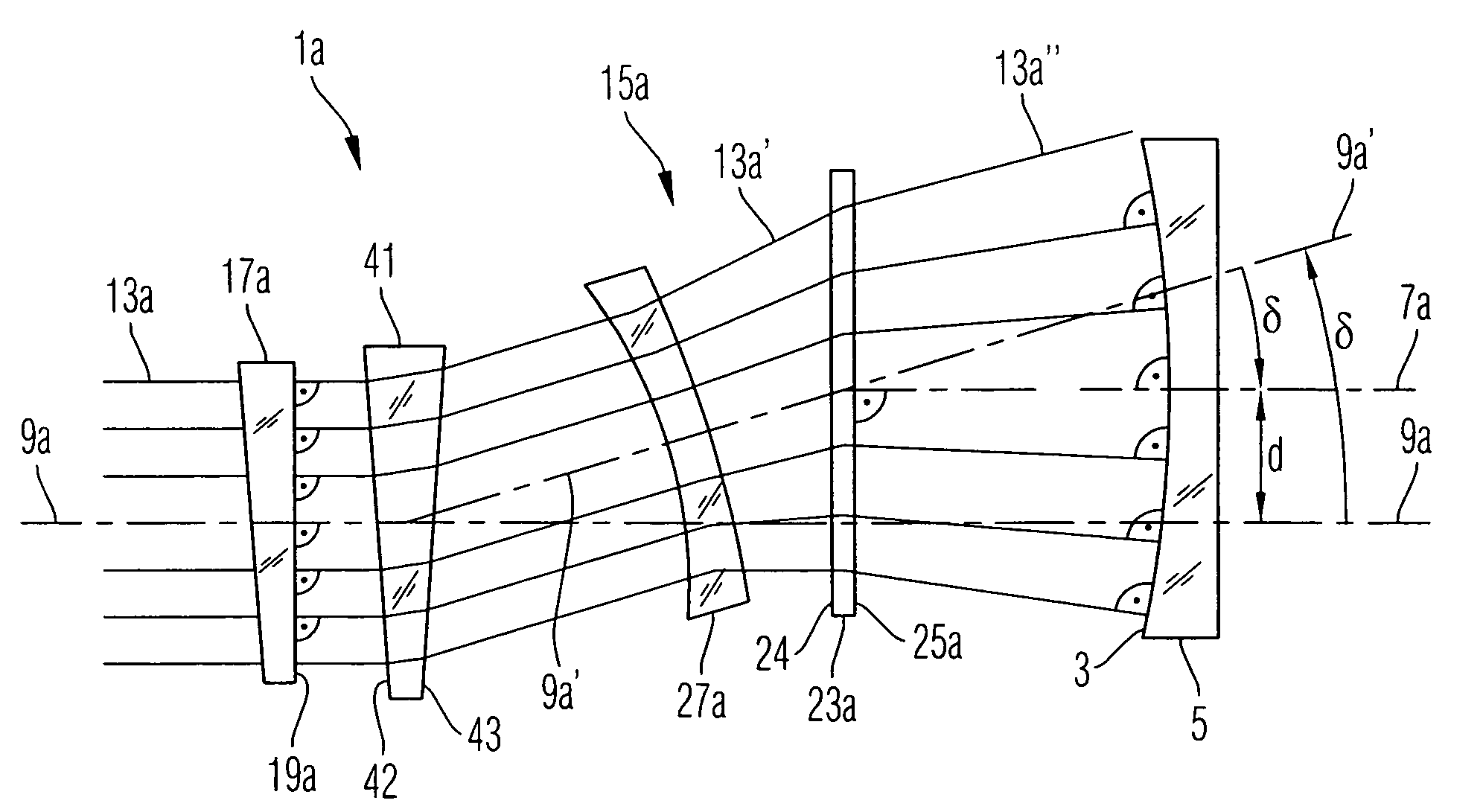
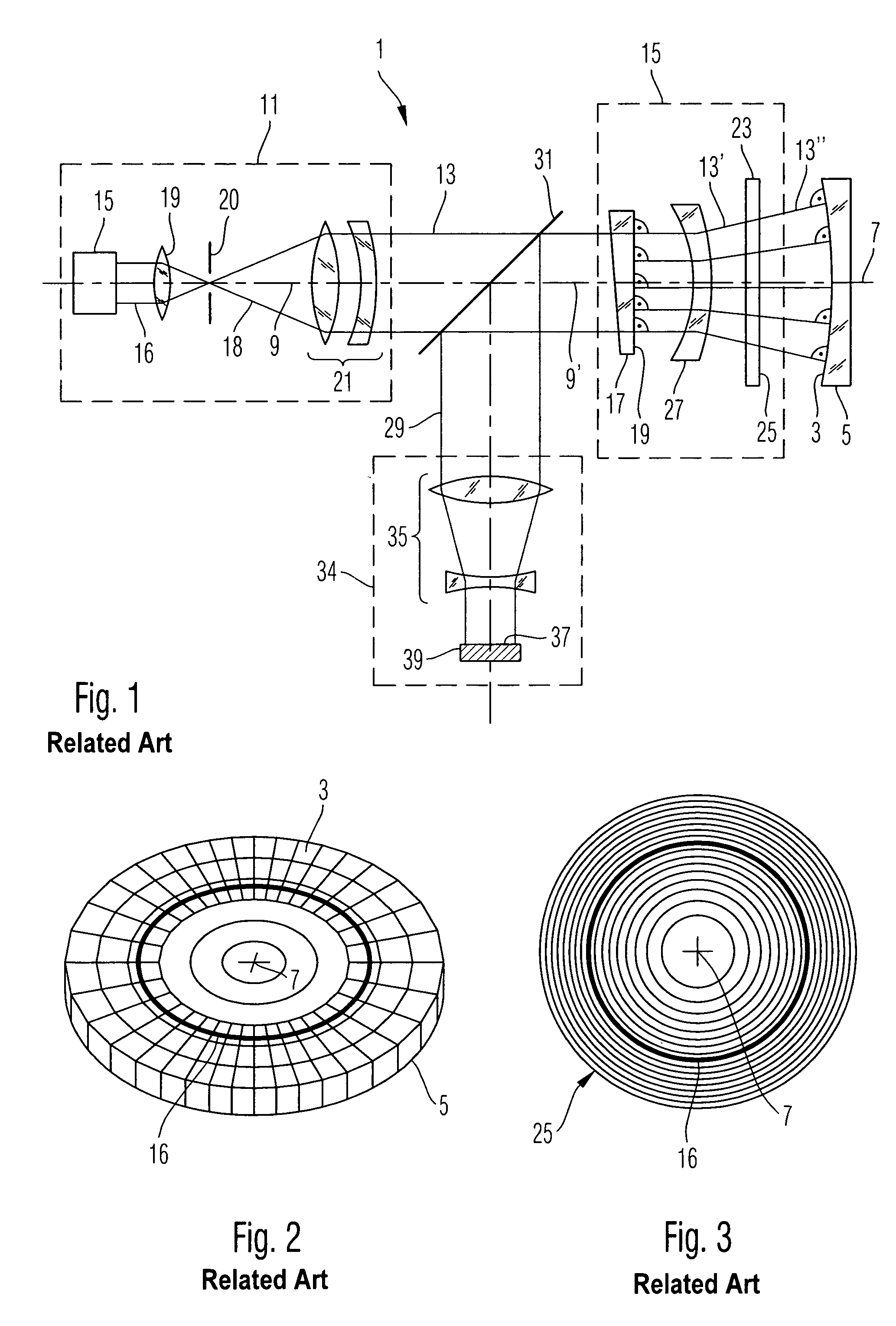
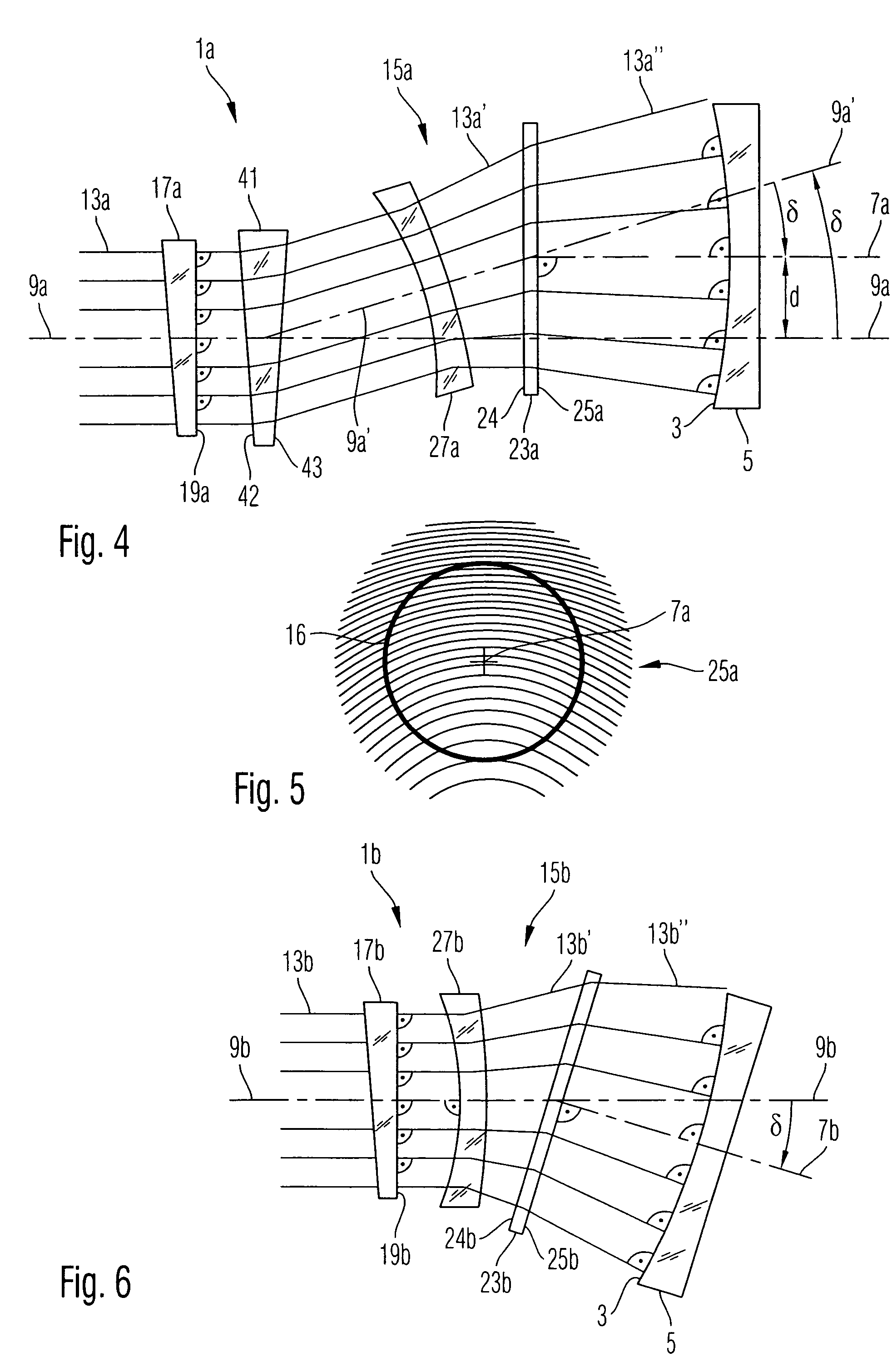
[0039]In the exemplary embodiments described below, components that are alike in function and structure are designated as far as possible by like reference numerals. Therefore, to understand the features of the individual components of a specific embodiment, the descriptions of other embodiments and of the summary of the invention should be referred to.

[0040]The exemplary embodiments of methods described below involve interferometrically taking measurements of wavefronts generated by reflecting an incident beam of measuring light provided by an interferometer apparatus from surfaces to be measured. Plural conventional interferometric methods may be used as a basis for taking such measurements. Examples of such interferometric methods are disclosed in e.g. U.S. Pat. No. 5,361,312, U.S. Pat. No. 5,982,490 and U.S. 2002 / 0063867 A1. The entire contents of these patents and publications are incorporated herein by reference.

[0041]For illustrating the particularities of embodiments of the ...


PUM


Abstract

A method of manufacturing an optical element having an optical surface of a target shape includes performing an interferometric test using an interferometer optics, wherein the interferometer optics includes a hologram that deflects a beam of measuring light by a substantial angle or that displaces an axis of symmetry of measuring light emerging from the hologram with respect to an axis of symmetry of measuring light incident on the hologram.

Description

BACKGROUND OF THE INVENTION[0001]1. Field of the Invention[0002]The present invention relates to a method of manufacturing an optical element. In particular, the invention relates to a method of manufacturing an optical element having an optical surface having a rotational symmetry, and in particular, the optical surface may have an aspherical shape.[0003]2. Brief Description of Related Art[0004]The optical element having the optical surface is, for example, an optical component such as an optical lens or an optical mirror used in optical systems, such as telescopes used in astronomy, and systems used for imaging structures, such as structures formed on a mask or reticle, onto a radiation sensitive substrate, such as a resist, in a lithographic method. The success of such an optical system is substantially determined by the accuracy with which the optical surface can be machined or manufactured to have a target shape determined by a designer of the optical system. In such manufactur...

Claims


Application Information

Patent Timeline
IPC IPC(8): G01B9/02
CPCG01B9/021G03H2001/0072G03H1/08G02B5/32
Inventor SCHILLKE, FRANKBEDER, SUSANNEHETZLER, JOCHEN
Owner CARL ZEISS SMT GMBH
Why Eureka
Try Eureka