MEMs device with feedback control

Active Publication Date: 2006-06-13
HEWLETT PACKARD DEV CO LP
View PDF4 Cites 25 Cited by
  • Summary
  • Abstract
  • Description
  • Claims
  • Application Information

AI Technical Summary

Benefits of technology

[0002]A MEMS device includes at least one movable member and an active device having at least one property affected by the location of the movable member with re

Problems solved by technology

However, this form of electrostatic control has snap-in issues when the controllable gaps are reduced below a threshold limit.
Conventional devices incorporate

Method used


Image

  • MEMs device with feedback control
  • MEMs device with feedback control
  • MEMs device with feedback control

Examples


Embodiment Construction

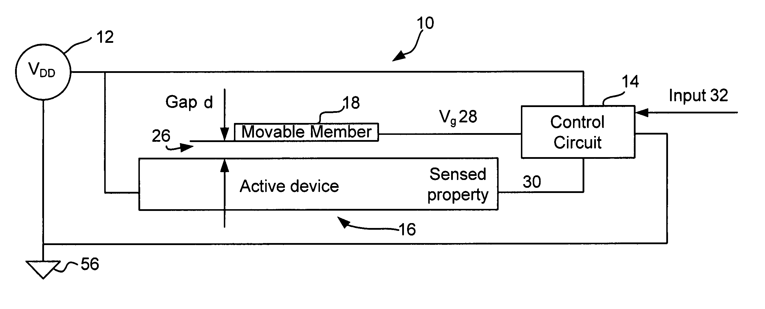
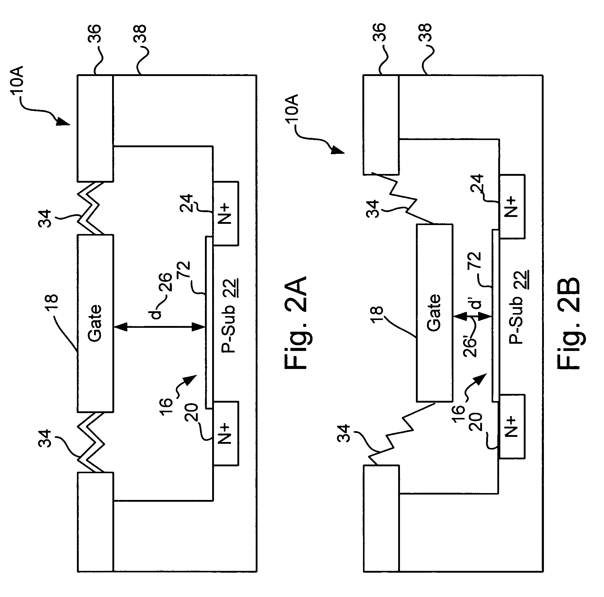
[0020]The MEMs devices of the present invention are applicable to a broad range of semiconductor, thin and thick film device technologies and can be fabricated from a variety of semiconductor technology related materials. The following description discusses several presently preferred embodiments of the MEMs and active devices of the present invention as implemented in silicon substrates, since the majority of currently available semiconductor devices are fabricated in silicon substrates and the most commonly encountered applications of the present invention will involve silicon substrates. Nevertheless, the present invention may also advantageously be employed in gallium arsenide, germanium, and other semiconductor materials. In addition, the present invention is not intended to be limited to those devices fabricated in silicon semiconductor materials, but will include those devices fabricated in one or more of the available MEMs and semiconductor related materials and technologies...


PUM


Abstract

A MEMS device includes at least one movable member and an active device having at least one property affected by the location of the movable member with respect to the active device. A control circuit is used to limit movement of the movable member based on observation of the property affected by the active device.

Description

BACKGROUND OF THE INVENTION[0001]Electrostatic micro-electromechanical (MEMs) devices typically are fabricated with semiconductor or other thin and thick film technologies. The MEMs devices often times have electrostatic actuators that are used to control various functions in display devices, high precision position sensors, pressure sensors, voltage modulators, accelerometers, oscillators, and adaptive optics, just to name a few. Electrostatic actuation is generally performed using a constant voltage source as the implementation of the control is less complicated than other methods. However, this form of electrostatic control has snap-in issues when the controllable gaps are reduced below a threshold limit. Further, if a gap separates two different metal plates and the gap is removed by allowing the two metal plates to contact each other, striction forces can prevent the two metal plates from becoming separated. Conventional devices incorporate mechanical stops to limit the gap dis...

Claims


Application Information

Patent Timeline
IPC IPC(8): G02B26/00
CPCG02B26/001G02B26/0833G09G3/3433H01L31/0232G09G3/346G09G3/3466G09G2320/029G09G2320/0295G09G2360/147H01L31/02162G09G2300/0819
Inventor CHEN, ZHIZHANGLIAO, HANGRAMAMOORTHI, SRIRAMMYERS, TIMOTHY F.
Owner HEWLETT PACKARD DEV CO LP
Why Eureka
Try Eureka