Magnetic random access memory array with thin conduction electrical read and write lines

a random access, magnetic technology, applied in the direction of digital storage, semiconductor devices, instruments, etc., can solve the problems of increasing the size of the required switching field, bringing with it its own problems, and causing significant problems, so as to reduce the high current, increase the switching field at the free layer, and achieve exceptional thinness

Inactive Publication Date: 2006-06-27
HEADWAY TECH INC +1
View PDF12 Cites 48 Cited by
  • Summary
  • Abstract
  • Description
  • Claims
  • Application Information

AI Technical Summary

Benefits of technology

[0009]Some degree of anisotropy is necessary if an MTJ cell is to be capable of maintaining a magnetization direction and, thereby, to effectively store data even when write currents are zero. As cell sizes have continued to decrease, the technology has sought to provide a degree of magnetic anisotropy by forming cells in a wide variety of shapes (eg. rectangles, diamonds, ellipses, etc.), so that the lack of inherent crystalline anisotropy is countered by a shape anisotropy. Yet this form of anisotropy brings with it its own problems. A particularly troublesome shape-related problem in MTJ devices results from non-uniform and uncontrollable edge-fields produced by shape anisotropy (a property of non-circular samples). As the cell size decreases, these edge fields become relatively more important than the magnetization of the body of the cell and have an adverse effect on the storage and reading of data. Although such shape anisotropies, when of sufficient magnitude, reduce the disadvantageous effects of super-paramagnetism, they have the negative effect of requiring high currents to change the magnetization direction of the MTJ for the purpose of storing data.
[0010]One way of addressing the problem of the high currents needed to change the magnetization direction of a free layer when its shape anisotropy is high, is to provide a mechanism for concentrating the fields produced by lower current values. This approach was taken by Durlam et al. (U.S. Pat. No. 6,211,090 B1) who teach the formation of a flux concentrator, which is a soft magnetic (NiFe) layer formed around a copper damascene current carrying line. The layer is formed around three sides of the copper line which forms the digit line at the underside of the MRAM cell.
[0011]Two additional approaches are taught by Nakao, (U.S. Pat. No. 6,509,621 B2), who, in one embodiment, forms a pinned layer out of a material that produces a high percentage of spin polarized electrons in the current and in another embodiment, applies an offsetting magnetic field produced by a magnetic shield to assist in causing field reversals in the cell element.
[0012]Yet another approach is taught by Sekiguchi et al., (U.S. Pat. No. 6,611,455 B2) who forms free layers with easy axes that are perpendicular to the layer plane, then forms word and bit lines in the same plane.
[0013]The present invention also addresses the problem of reducing the high current required to reorient the magnetization of the free layer in ultra-small MRAM cells wherein the super-paramagnetic behavior requires thick free layers. It does so by forming word and / or bit lines of exceptional thinness, specifically under 100 nm, compared to conventional thicknesses of approximately 300 nm, thereby increasing the switching field at the free layer by as much as a factor of 2. An additional benefit of such thin lines is the ease of their fabrication. The patterning process for their formation requires the removal of less material and can eliminate the need for chemical mechanical polishing (CMP), which can produce uncontrollable variations in line thicknesses. Finally, these ultra-thin lines are easily formed into a variety of configurations with respect to their positions relative to the MTJ cell. In the present invention the cell is positioned between the word and bit lines. In the following description the general method of forming the lines will be described along with illustrations of their placement relative to the cell.SUMMARY OF THE INVENTION
[0014]A first object of this invention is to provide an MTJ MRAM cell that makes more efficient use of word and bit line switching currents, the lines thereby producing magnetic fields of sufficient intensity for switching, while requiring lower currents to do so.

Problems solved by technology

Parkin also notes that such small sizes are associated with significant problems, particularly super-paramagnetism, which is the spontaneous thermal fluctuation of magnetization in samples of ferromagnetic material too small to have sufficient magnetic anisotropy (a measure of the ability of a sample to maintain a given magnetization direction).
Unfortunately, the size of the required switching field increases with layer thickness, so the price paid for a thermally stable cell is the necessity of expending a great deal of current to change the magnetic orientation of the cell's free layer.
Yet this form of anisotropy brings with it its own problems.
A particularly troublesome shape-related problem in MTJ devices results from non-uniform and uncontrollable edge-fields produced by shape anisotropy (a property of non-circular samples).
As the cell size decreases, these edge fields become relatively more important than the magnetization of the body of the cell and have an adverse effect on the storage and reading of data.
Although such shape anisotropies, when of sufficient magnitude, reduce the disadvantageous effects of super-paramagnetism, they have the negative effect of requiring high currents to change the magnetization direction of the MTJ for the purpose of storing data.

Method used


Image

  • Magnetic random access memory array with thin conduction electrical read and write lines
  • Magnetic random access memory array with thin conduction electrical read and write lines
  • Magnetic random access memory array with thin conduction electrical read and write lines

Examples


Embodiment Construction

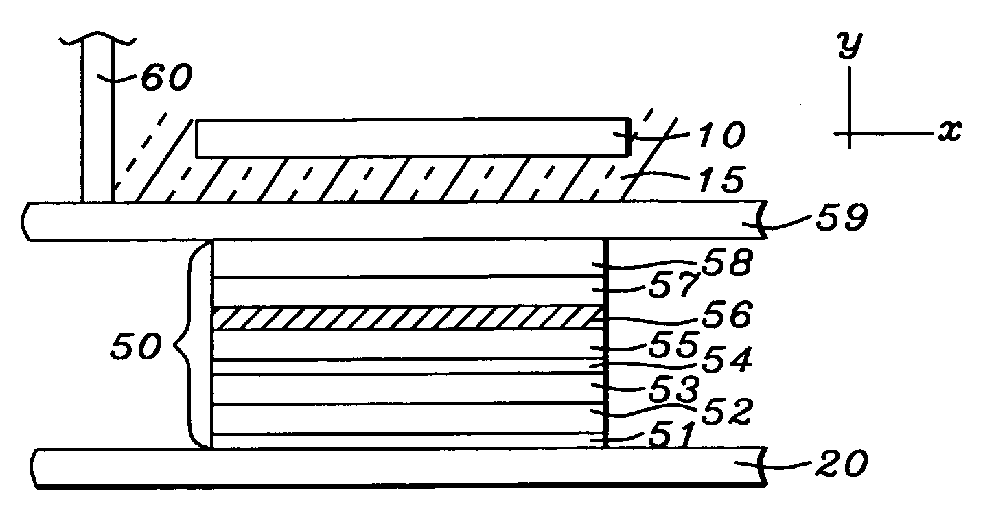
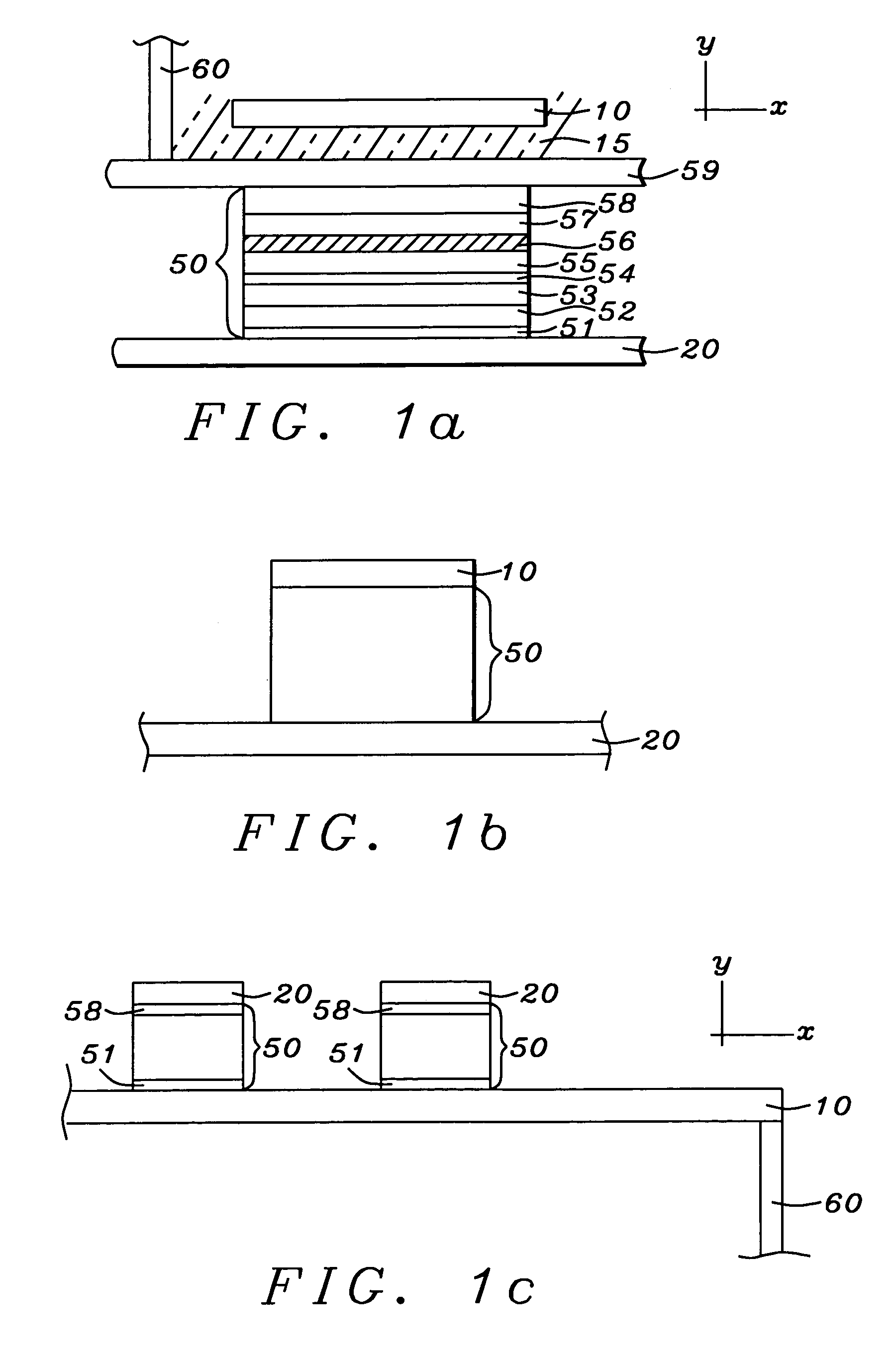
[0027]The preferred embodiment of the present invention is an MTJ MRAM cell formed at an intersection of ultra-thin word and bit lines, more specifically between those lines, so that smaller currents can still produce adequate switching fields at the location of the cell free layer.

[0028]Referring again to FIG. 1a, there is shown the multi-layered MTJ cell element (50) formed between orthogonally directed, vertically separated ultra-thin word (10) and bit (20) lines of the invention. The two lines extend in vertically separated horizontal planes, crossing over each other but insulated from each other and forming, thereby, an intersection at which the cell is located. In all that follows, the term “intersection” is taken to mean a vertically separated crossing of lines. The word line is directed perpendicularly out of the figure plane, the bit line is within the figure plane. An additional conducting electrode, (alternatively denoted a read-word line), used in read operations (59), i...


PUM


Abstract

An MTJ MRAM cell is formed between ultra-thin orthogonal word and bit lines of high conductivity material whose thickness is less than 100 nm. Lines of this thickness produce switching magnetic fields at the cell free layer that are enhanced by a factor of approximately two for a given current. The fabrication of a cell with such thin lines is actually simplified as a result of the thinner depositions because the fabrication process eliminates the necessity of removing material by CMP during patterning and polishing, thereby producing uniform spacing between the lines and the cell free layer.

Description

RELATED PATENT APPLICATIONS[0001]This Application is related to Ser. No. 10 / 910,725, filed on Aug. 3, 2004 and assigned to the same assignee as the present application.BACKGROUND OF THE INVENTION[0002]1. Field of the Invention[0003]This invention relates to the design and fabrication of magnetic tunnel junctions (MTJ) as memory storage devices, particularly to a design wherein word and bit lines are ultra-thin so as to produce higher magnetic flux at the MTJ free layer for a given write current.[0004]2. Description of the Related Art[0005]The magnetic tunnel junction (MTJ) basically comprises two electrodes, which are layers of magnetized ferromagnetic material, separated by a tunnel barrier layer, which is a thin layer of insulating material. The tunnel barrier layer must be sufficiently thin so that there is a probability for charge carriers (typically electrons) to cross the layer by means of quantum mechanical tunneling. The tunneling probability is spin dependent, however, beca...

Claims


Application Information

Patent Timeline
Patent Type & Authority Patents(United States)
IPC IPC(8): H01L21/00
CPCG11C11/16G11C11/1659G11C11/161G11C11/1657G11C5/02H10B61/00H10N50/01
Inventor MIN, TAIWANG, POKANGSHI, XIZENGGUO, YIMIN
Owner HEADWAY TECH INC
Why Eureka
Try Eureka