
Control of a photosensitive cell

a photosensitive cell and control technology, applied in the field of photosensitive cells, can solve the problem of becoming difficult to ensure a good charge transfer from photodiode d/sub>2 to read node s

Active Publication Date: 2006-06-27
STMICROELECTRONICS SRL
View PDF3 Cites 17 Cited by
  • Summary
  • Abstract
  • Description
  • Claims
  • Application Information

AI Technical Summary

Benefits of technology

[0015]The present invention provides a method and a device for controlling a photosensitive cell enabling ensuring complete transfer of the charges from the photodiode to the read node.

Problems solved by technology

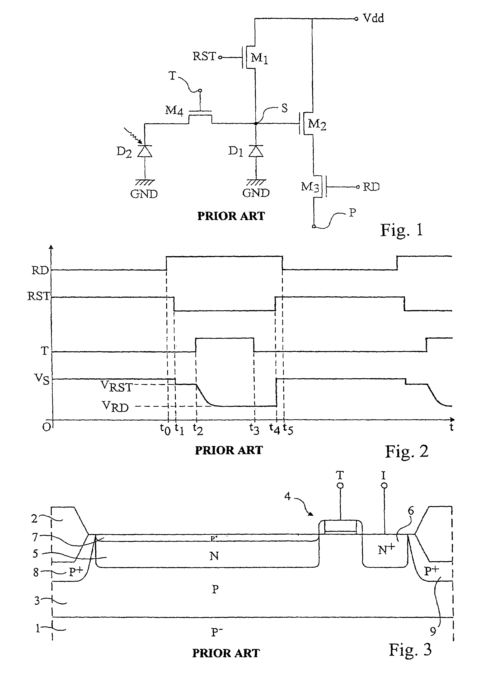
For denser and denser technologies with photosensitive cells of small dimensions and lower and lower control signals, it becomes difficult to ensure a good charge transfer from photodiode D2 to read node S.
This may translate as an error on the measured wanted signal level VRD and result in a so-called “trailing” effect upon successive readings of a photosensitive cell, due to the reading of residual charges of the previous image upon reading of the next image.

Method used


Image

  • Control of a photosensitive cell
  • Control of a photosensitive cell
  • Control of a photosensitive cell

Examples


Embodiment Construction

[0035]The same elements have been referred to with the same reference numerals in the different drawings and, further, as usual in the representation of integrated circuits, FIG. 3 is not drawn to scale.

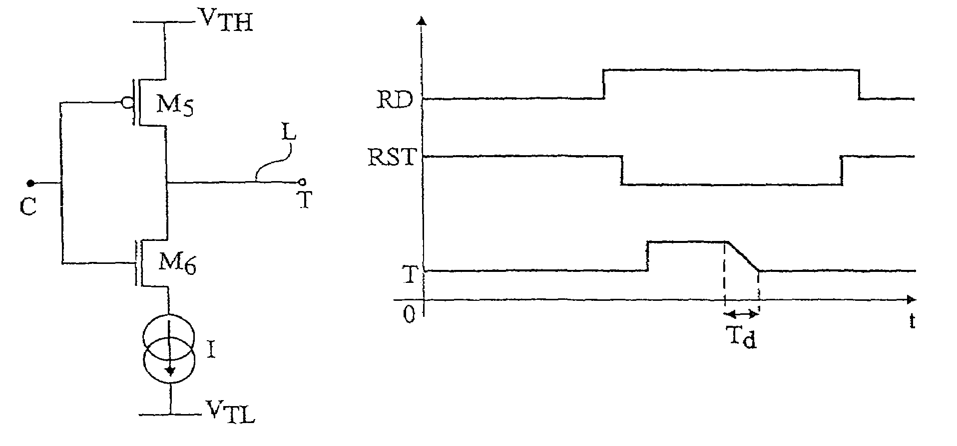
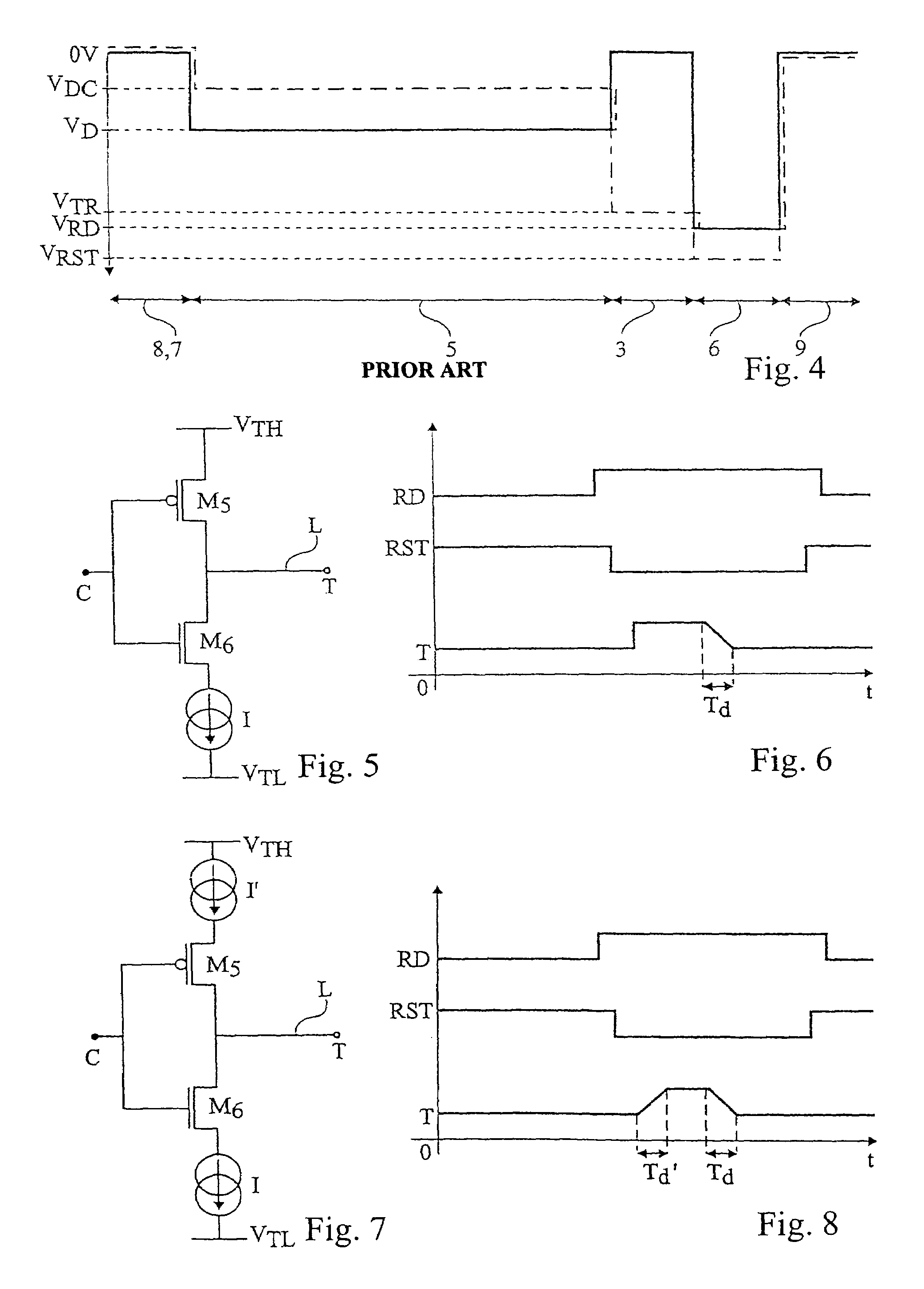
[0036]The present invention comprises providing a charge transfer control signal T having a determined average slope upon transition between the high level and the low level to enable complete transfer of the charges between photodiode D2 and read node S.

[0037]FIG. 5 shows a first embodiment of the last stage of a control circuit providing charge transfer control signal T to the gate of transfer transistor M4. The control circuit may be connected to a line L connected to all the transfer transistor gates of the photosensitive cells of a same photosensitive cell row. The control circuit comprises a P-type MOS transistor M5 having its drain connected to a high-level voltage source VTH and having its source connected to line L. The control circuit comprises an N-type MOS transistor M6 h...


PUM


Abstract

A device and a method for controlling a photosensitive cell including a photodiode adapted to discharging into a read node via a MOS transfer transistor, the device being adapted to providing a signal for controlling the gate of the MOS transfer transistor to a first level for which the MOS transfer transistor is off or to a second level for which the MOS transfer transistor is on, including means for providing a transition control signal between the second level and the first level of determined average slope.

Description

BACKGROUND OF THE INVENTION[0001]1. Field of the Invention[0002]The present invention relates to the control of a photosensitive cell made in monolithic form of an image sensor intended to be used in shooting devices such as, for example, shooting cameras, camcorders, digital microscopes, or digital cameras. More specifically, the present invention relates to a photosensitive cell based on semiconductors.[0003]2. Discussion of the Related Art[0004]FIG. 1 schematically shows the circuit of a photosensitive cell of a photosensitive cell array of an image sensor. With each photosensitive cell of the array are associated a precharge device and a read device. The precharge device is formed of an N-channel MOS transistor M1, interposed between a supply rail Vdd and a read node S. The gate of precharge transistor M1 receives a precharge control signal RST. The read device is formed of the series connection of two N-channel MOS transistors, M2, M3. The drain of first read transistor M2 is c...

Claims


Application Information

Patent Timeline
Patent Type & Authority Patents(United States)
IPC IPC(8): G01J1/44H01J40/14H01L31/00H03F3/08H01L27/146H04N25/65
CPCH01L27/14601H04N5/374H04N5/363H04N25/65H04N25/76
Inventor CAZAUX, YVONROY, FRANCOIS
Owner STMICROELECTRONICS SRL
Learn More