Semiconductor integrated circuit device

a technology of integrated circuits and semiconductors, applied in the direction of semiconductor devices, electrical equipment, transistors, etc., can solve the problems of control devices not functioning normally, interfering with the normal operation of motors, etc., and achieve the effect of more reliable conclusion

Active Publication Date: 2006-06-27
SEMICON COMPONENTS IND LLC
View PDF5 Cites 28 Cited by
  • Summary
  • Abstract
  • Description
  • Claims
  • Application Information

AI Technical Summary

Benefits of technology

[0007]The present invention has been made in consideration of the foregoing problems. A semiconductor integrated circuit device according to the invention includes a plurality of opposite-conductivity-type epitaxial layers deposited on a single-conductivity-type semiconductor substrate, and dividing regions dividing the epitaxial layers into a plurality of island regions. The island regions comprising at least an-sland region incorporating a driver device for driving a motor and at least another island region incorporating a control device for controlling the driver device. A device formed region in the island region having the control device has an opposite-conductivity-type embedded diffusion region between the substrate and a first epitaxial layer deposited on an upper surface of the substrate and a grounded single-conductivity-type embedded diffusion region on the first epitaxial layer. Accordingly, the semiconductor integrated circuit device according to the invention has an opposite-conductivity-type embedded diffusion region between the substrate and the first epitaxial layer in the island region having a control device, and a grounded single-conductivity-type embedded diffusion region on an upper surface of the opposite-conductivity-type embedded diffusion region. Thus free carriers (electrons) generated from the driver device by the back electromotive force of the motor are attracted through the opposite-conductivity-type diffusion region, thus being prevented from flowing into the control device. This prevents the malfunction of the control device due to the free carriers (electrons) generated from the driver device. The single-conductivity-type embedded diffusion region serves as the substrate of the control device.
[0010]The semiconductor integrated circuit device according to the invention includes a plurality of opposite-conductivity-type epitaxial layers deposited on a single-conductivity-type semiconductor substrate, and dividing regions dividing the substrate and the epitaxial layers into a plurality of island regions. The island regions comprising at least an island region incorporating a driver device for driving a motor and at least another island region incorporating a control device for controlling the driver device. The island region having the driver device has an opposite-conductivity-type embedded diffusion region between the substrate and a first epitaxial layer deposited on an upper surface of the substrate and a grounded single-conductivity-type embedded diffusion region on the first epitaxial layer. Accordingly, the semiconductor integrated circuit device of the invention has an opposite-conductivity-type embedded diffusion region between the substrate and the first epitaxial layer in the island region having a driver device, and a grounded single-conductivity-type embedded diffusion region on an upper surface of the opposite-conductivity-type embedded diffusion region. Thus the free carriers (electrons) generated from the driver device by the back electromotive force of the motor are attracted through the opposite-conductivity-type diffusion region, thus being prevented from flowing into the control device. This prevents the malfunction of the control device due to the free carriers (electrons) generated from the driver device. The single-conductivity-type embedded diffusion region serves as the substrate of the driver device.
[0011]The semiconductor integrated circuit device according to the invention includes an island region having a motor-driving device and an island region having a control device for controlling the driver device. A device formed region in the island region having the control device is separated from the substrate by an opposite-conductivity-type embedded diffusion region having supply potential. Thus free carriers (electrons) generated from the PN junction of the driver device by the back electromotive force of the motor are prevented from flowing into the control device by the single-conductivity-type embedded diffusion region. Thus the malfunction of the control device due to the free carriers (electrons) can be prevented and as such, the malfunction of the driver device can be prevented.
[0012]The semiconductor integrated circuit device according to the invention includes multiple epitaxial layers on the upper surface of the substrate in the island region having the control device. An opposite-conductivity-type embedded diffusion region having supply potential is disposed between the substrate and the first epitaxial layer. A single-conductivity-type embedded diffusion region is disposed between the first epitaxial layer and an epitaxial layer thereon. The single-conductivity-type embedded diffusion region connects to the dividing region in the island region having the control device. Thus, a grounded single-conductivity-type embedded diffusion region is disposed on the opposite-conductivity-type embedded diffusion region, so that the single-conductivity-type embedded diffusion region can be the diffusion region of a desired impurity concentration. Accordingly, the single-conductivity-type embedded diffusion region can be grounded more reliably and so it serves as the substrate, so that a latch-up phenomenon in the control device can be prevented.
[0013]In the semiconductor integrated circuit device according to the invention, the opposite-conductivity-type embedded diffusion region which prevents the free carriers (electrons) generated from the driver device from flowing into the control device and the single-conductivity-type embedded diffusion region which prevents the latch-up phenomenon in the control device are disposed separately in different regions. The embedded diffusion regions can therefore have respective desired impurity concentrations, thus having respective advantages.

Problems solved by technology

Particularly, when the free carriers (electrons) flow into the control device for controlling the driver device, the control device fails to function normally.
This causes the driver device which should be in OFF action to make ON action to send an incorrect signal, thus interfering with the normal operation of the motor.

Method used


Image

  • Semiconductor integrated circuit device
  • Semiconductor integrated circuit device
  • Semiconductor integrated circuit device

Examples


Embodiment Construction

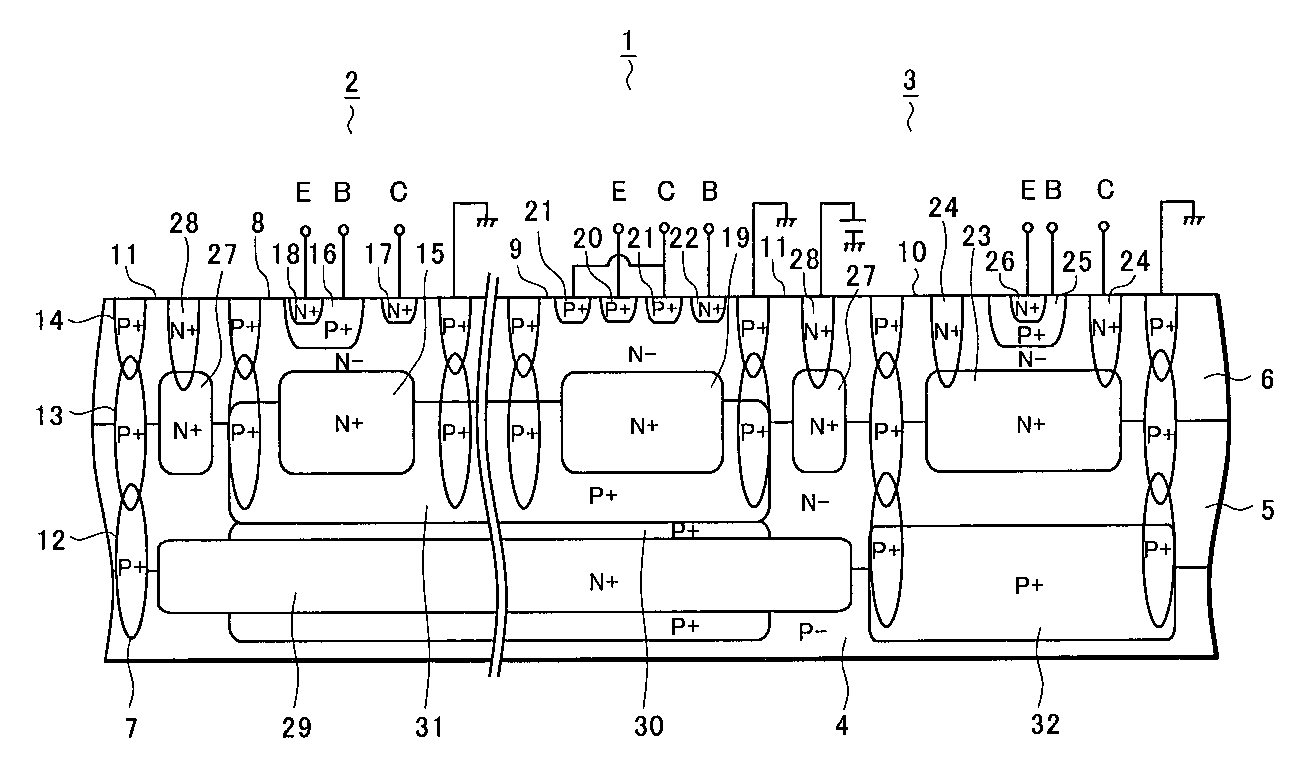
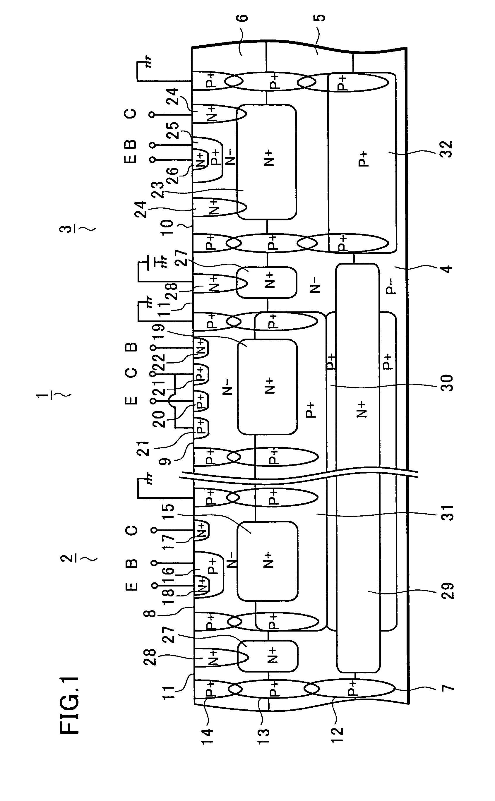
[0020]A semiconductor integrated circuit device according to embodiments of the invention will be specifically described with reference to FIGS. 1 to 6.

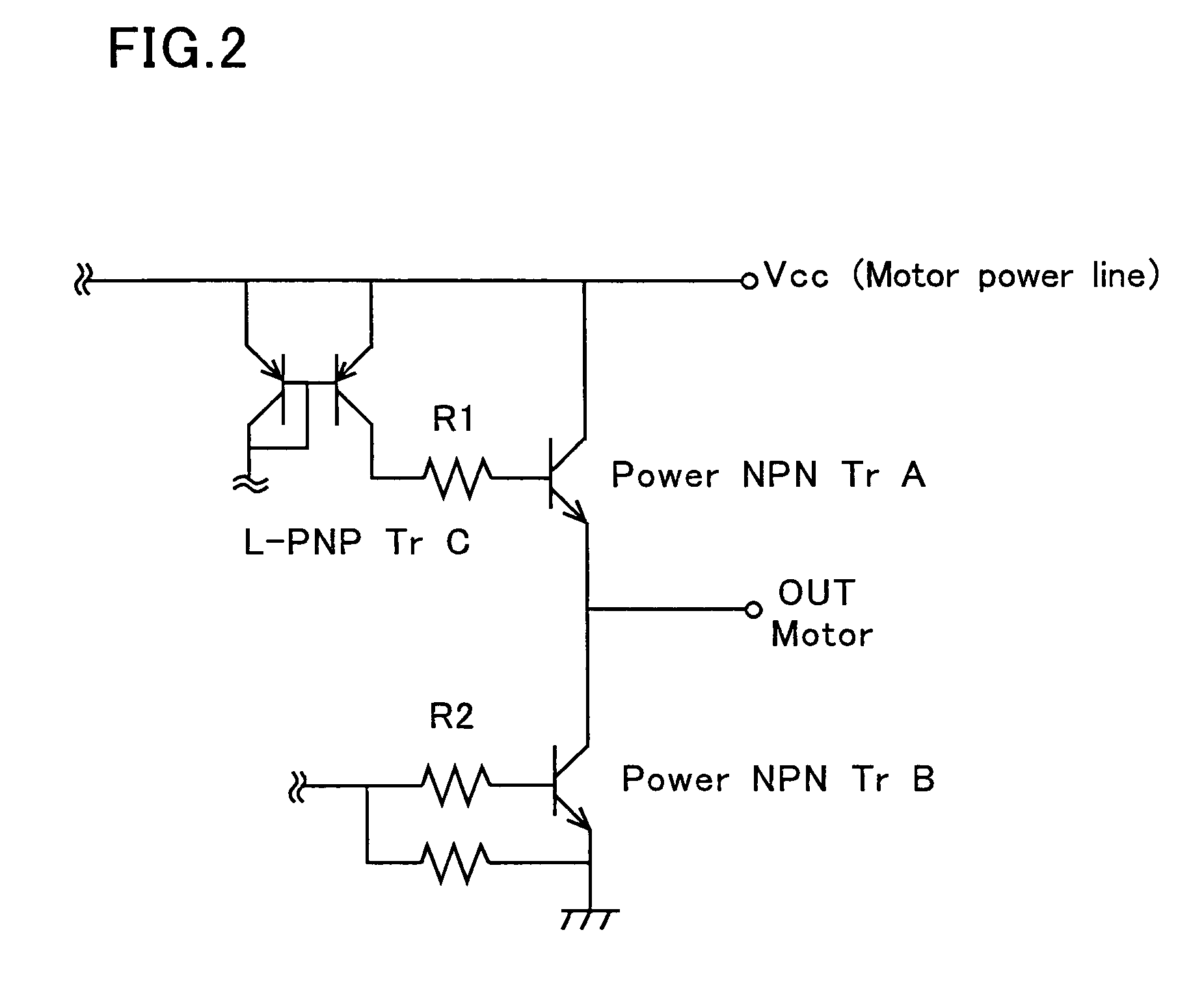
[0021]FIGS. 1 and 3 to 6 are cross-sectional views of the semiconductor integrated circuit device according to embodiments of the invention. FIG. 2 is part of the circuit diagram of the semiconductor integrated circuit device according to the embodiment of the invention.

[0022]Referring to FIG. 1, a first N-type epitaxial layer 5 in a thickness of, e.g., about 2 to 10 μm is formed on a P-type monocrystal silicon substrate 4. A second N-type epitaxial layer 6 in a thickness of, e.g., about 2 to 10 μm is formed on the first epitaxial layer 5. The substrate 4 and the first and second epitaxial layers 5 and 6 are divided into a first island region 8, a second island region 9, a third island region 10, and a fourth island region 11 by P-type dividing regions 7 which pass therethrough. Although not shown, the substrate 4 and the first and s...


PUM


Abstract

A semiconductor integrated circuit device according to the invention includes an N-type embedded diffusion region between a substrate and a first epitaxial layer in island regions serving as small signal section. The substrate and the first epitaxial layer are thus partitioned by the N-type embedded diffusion region having supply potential in the island regions serving as small signal section. This structure prevents the inflow of free carriers (electrons) generated from a power NPN transistor due to the back electromotive force of the motor into the small signal section, thus preventing the malfunction of the small signal section.

Description

BACKGROUND OF THE INVENTION[0001]1. Field of the Invention[0002]The present invention relates to a semiconductor integrated circuit device in which the malfunction of a motor drive circuit due to a parasitic effect is prevented.[0003]2. Description of the Related Art[0004]Conventional three-phase motor drivers have three parallel-connected transistors (Tr1–Tr2, Tr3–Tr4, and Tr5–Tr6) each connected in series between direct-current power supplies VCC and GND. Output terminals taken from between Tr1–Tr2, Tr3–Tr4, and Tr5–Tr6 are connected to a motor M. Thus, normal / back electromotive force is generated as the motor rotates / stops. It is proposed in the art to provide a structure in which a protective diode is connected between the collector and the emitter of the transistors to dissipate the electromotive force to a fixed potential, thereby protecting the interior of an IC including the series transistors (for example, refer to Patent Document: JP-A-6-104459, pp. 13–14, FIGS. 16–17).[00...

Claims


Application Information

Patent Timeline
Patent Type & Authority Patents(United States)
IPC IPC(8): H01L29/00H01L21/74H01L21/761H01L21/8222H01L21/8224H01L21/8226H01L21/8228H01L21/8248H01L21/8249H01L27/06H01L27/082H01L31/113
CPCH01L21/8224H01L27/0826H01L27/0821H01L27/0623H01L29/7816H01L29/1083H01L21/8249
Inventor KANDA, RYOOKAWA, SHIGEAKIYOSHITAKE, KAZUHIRO
Owner SEMICON COMPONENTS IND LLC
Why Eureka
Try Eureka