

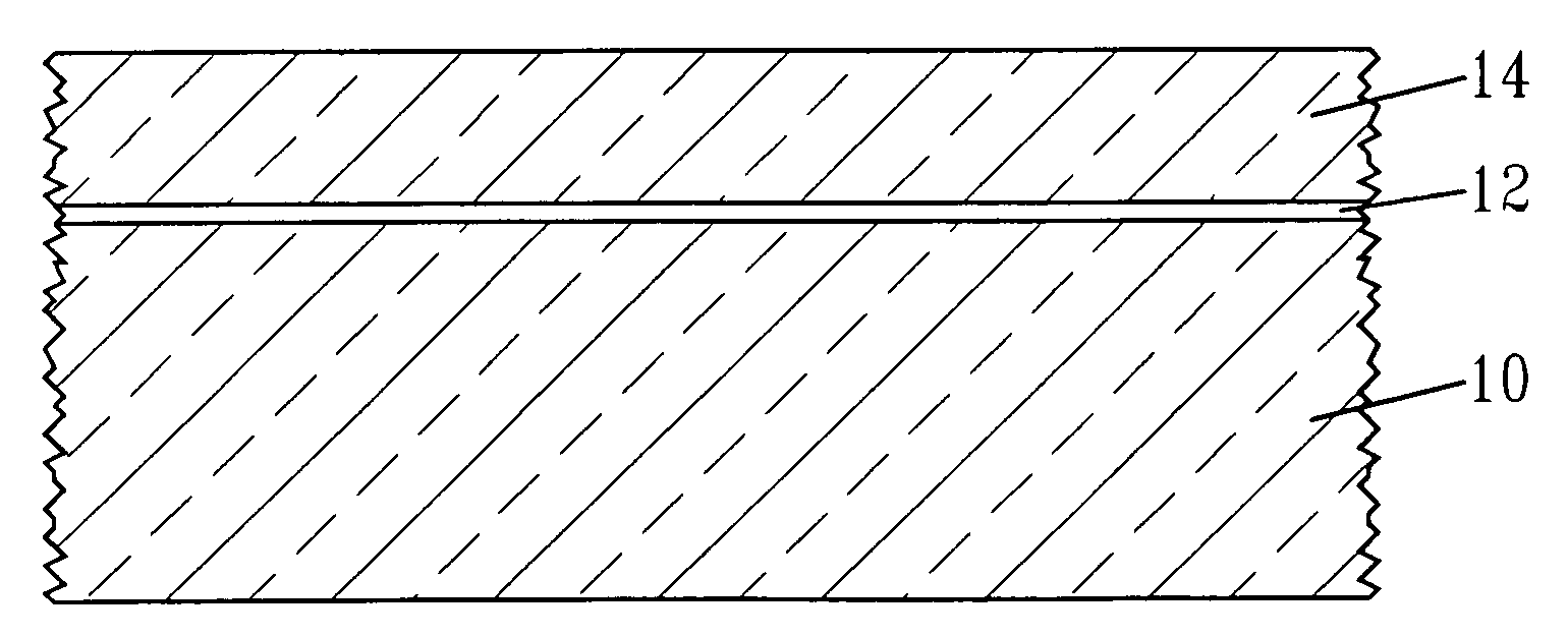
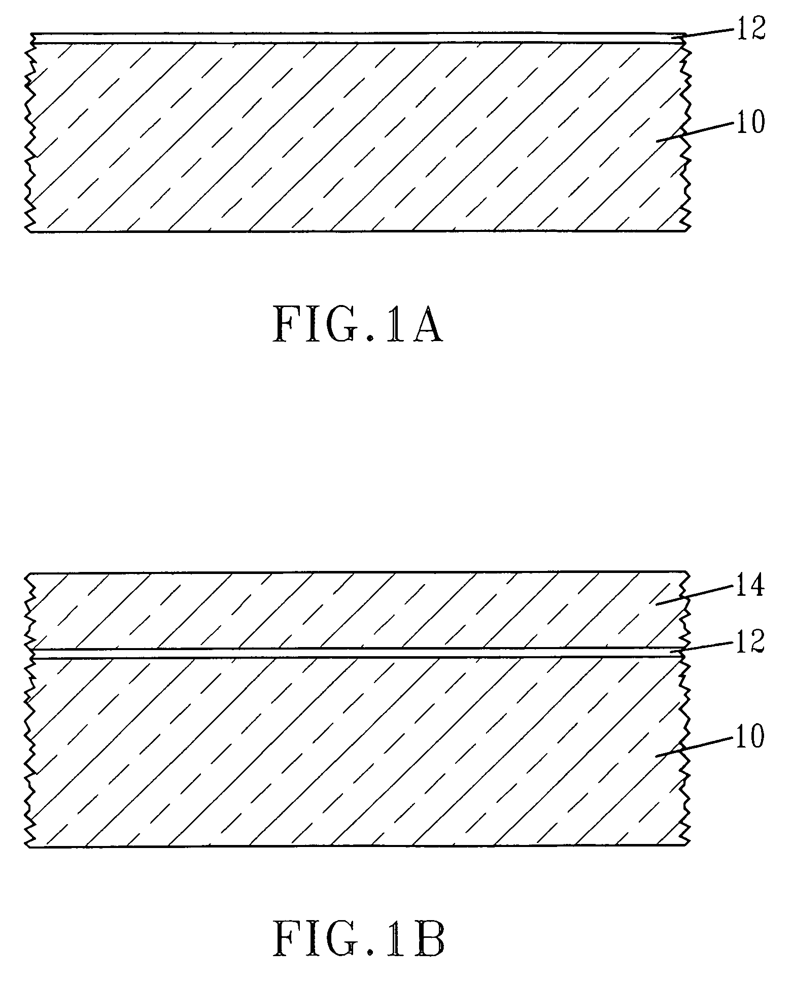
Chemical treatment to retard diffusion in a semiconductor overlayer
a technology of chemical treatment and overlayer, which is applied in the direction of semiconductor/solid-state device manufacturing, basic electric elements, electric apparatus, etc., can solve the problems of limiting the flexibility of process integration, limiting diffusion, and limiting the flexibility of diffusion
- Summary
- Abstract
- Description
- Claims
- Application Information
AI Technical Summary
Benefits of technology
Problems solved by technology
Method used
Image

Examples
example
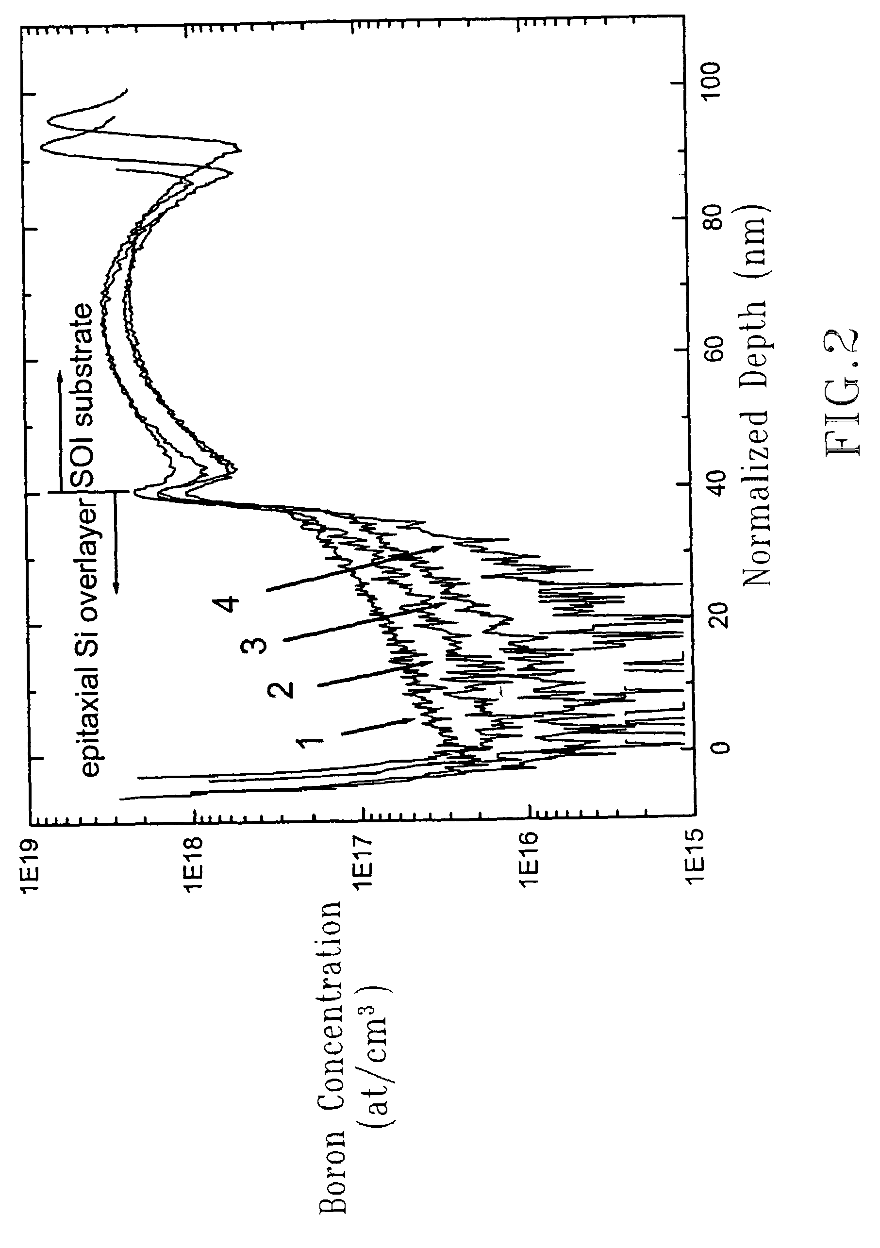
[0040]In this example, two silicon-on-insulator (SOI) substrates, each having an SOI layer that has a thickness of about 50 nm were employed. Each of the SOI substrates, in particular each SOI layer, was doped with boron by ion implantation using an ion dose of 2E13 B atoms / cm2 at 10 keV. The samples were then annealed at about 1000° C. for less than 10 seconds.
[0041]Each SOI substrate was then subjected to a step in which the SOI layer was hydrogen terminated. The hydrogen termination was provided by applying dilute hydrofluoric acid to each of the SOI substrates. After hydrogen termination, one of SOI substrates was soaked in a solution of 5×10⁻⁴ M iodine in methanol to provide a methoxy termination comprising carbon and oxygen to the SOI layer. The iodine / methanol soak occurred at room temperature for about 20 minutes. The soaked SOI substrate was then rinsed with methanol and dry utilizing a standard surface tension gradient drying process.
[0042]A Si layer having a thickness of ...
PUM
 Abstract
Description
Claims
Application Information