Wiring structure to minimize stress induced void formation

a technology of wiring structure and stress induced void, which is applied in the direction of semiconductor/solid-state device testing/measurement, radio frequency controlled devices, instruments, etc., can solve the problems of device failure, stress induced voiding is a common problem, and the device fails

Inactive Publication Date: 2006-01-26
TAIWAN SEMICON MFG CO LTD
View PDF21 Cites 21 Cited by
  • Summary
  • Abstract
  • Description
  • Claims
  • Application Information

AI Technical Summary

Benefits of technology

[0017] A preferred embodiment of the present invention provides a test structure for measuring via resistance that prevents or impedes vacancies in a void reservoir from migrating to the vicinity of a via and causing void formation.
[0019] Another preferred embodiment of the present invention provides an interconnect structure that is able to minimize a stress induced voiding phenomenon and thereby improve the reliability and product yield of a device having a conducting layer connected to a via.
[0020] Yet another preferred embodiment of the present invention incorporates a protrusion at one end of a conducting layer wherein the protrusion forms a connection to a via and has at least one bending portion and extension to delay the diffusion of vacancies to the via.
[0021] Yet another preferred embodiment of the present invention provides a method for forming an interconnect with an improved resistance to stress induced void formation.

Problems solved by technology

There is a significant challenge to improve the reliability of the final device because the repeated passage of current through an electrical circuit stresses the (metal) conductors and may induce voids that cause device failure.
Stress induced voiding is a common problem in multi-level interconnects, particularly those comprised of copper.
One leading cause of device failure is electromigration that forms a void by the movement of metal ions or vacancies in a conductive element as a result of a current passing through it.
Thus, a portion of the first conducting layer that is adjacent to the via 5 is especially susceptible to void formation due to electromigration.
When bump concentration at a given location is more than 20% higher than the average bump density, long term failure is predicted at that site.
Therefore when performing reliability testing on an interconnect, conventional test structures typically underestimate the lifetime before device failure occurs because they fail to account for voids in a bulk metal such as a bonding pad or a large area metal layer that diffuse through a narrow metal connection to a via.
Unfortunately, the reliability test underestimates the time before device failure since vacancies (not shown) in bond pad 11 migrate through metal line 13 to form a void (not shown) at the bottom of via 20 that increases via resistance R to an unacceptable level.
However, this intended remedy has its own drawbacks since this type of design will lead to a higher total resistance and more risk in the via manufacturing process.
The practice of adding more vias also increases the difficulty in checking the design rule.
However, the reservoir is not placed between the interconnect line and an adjoining via and therefore does not prevent vacancies from migrating within the interconnect to the via.
Unfortunately, the problem of vacancy accumulation on the upstream side of the via is not prevented.
Thus, an improved interconnect structure is required that overcomes the driving force for vacancies in a large area metal layer to migrate to the upstream side of a via and form a void that degrades device performance.

Method used


Image

  • Wiring structure to minimize stress induced void formation
  • Wiring structure to minimize stress induced void formation
  • Wiring structure to minimize stress induced void formation

Examples


first embodiment

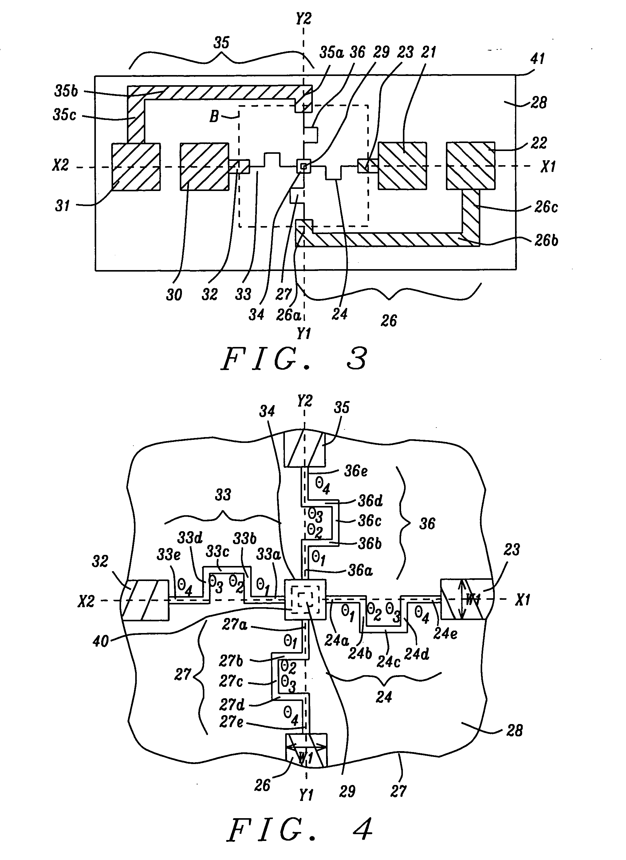
[0048] In the first embodiment depicted in FIGS. 3-7, a via test structure formed on a semiconductor substrate is used to measure via resistance and is particularly useful for providing a more accurate determination of the lifetime of a via during a reliability stress test. The present invention also provides for a method that employs the novel via test structure to determine via resistance during a reliability stress test.

[0049] Referring to FIG. 3, a top-down view of the via test structure of a preferred embodiment of the present invention is shown. Via test structure 41 is fabricated on a semiconductor substrate (not shown) which is typically silicon but may also be based on other semiconductor materials used in the art. The via test structure 41 is formed in layer 28 that may be either a homogenous layer or may include one or more etch stop layers, one or more low k dielectric layers, and one or more cap or passivation layers. Individual dielectric layers within the dielectric l...

second embodiment

[0071] In a second embodiment depicted in FIGS. 11-12, a wiring structure is formed on a substrate and is comprised of a first conducting layer having a large area portion with a first thickness, a first width, a first length, and a plurality of sides and a protrusion having a first thickness, second width, and second length with two ends and at least one bending portion. One end of the protrusion is connected to one side of the large area portion while the other end is connected to the bottom of a via that adjoins an overlying second conducting layer.

[0072] Referring to FIG. 11, a method of forming the first conducting layer in the interconnect structure of the present invention is described. A substrate 57 is shown upon which an etch stop layer 58 and a dielectric layer 59 have been sequentially deposited by a chemical vapor deposition (CVD) method, plasma enhanced CVD (PECVD) method, or the like. The substrate 57 is typically comprised of silicon and may include active and passiv...

third embodiment

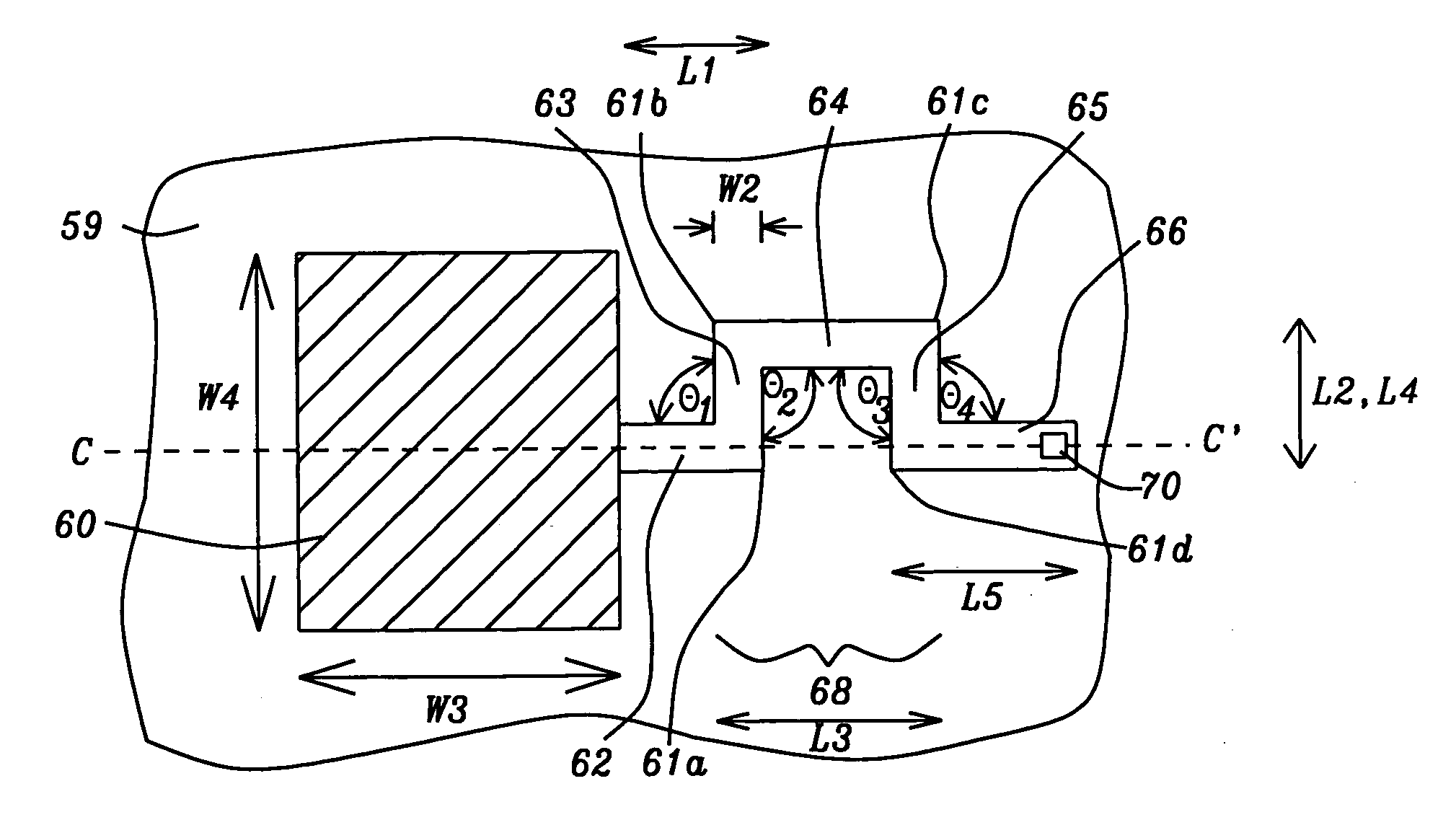
[0077] Referring to FIG. 12, a third embodiment is depicted in which the protrusion that connects a large area portion with a via in a first conducting layer is comprised of five segments and one bending portion that has three segments. The first conducting layer is comprised of the large area portion 60 having a first width w3, a first length w4, and a first thickness and a protrusion that has five overlapping segments each having a width w2, a length, two ends, and a first thickness. The first segment 62, second segment 63, and third segment 64 are formed substantially as described above. One end of a fourth segment 65 with a length MA overlaps the end of the third segment 64 that does not overlap the second segment 63 to form a bend 61c with an angle θ3 of about 45° to 135°. There is a fifth segment 66 with an end that overlaps the other end of the fourth segment 65 to form a bend 61d with an angle θ4 of about 45° to 135°. The fifth segment 66 that has a length L5 is preferably f...


PUM


Abstract

A wiring structure with improved resistance to void formation and a method of making the same are described. The wiring structure has a first conducting layer that includes a large area portion which is connected to an end of a protrusion with a plurality of “n” overlapping segments and at least one bending portion. The other end of the protrusion is connected to the bottom of a via which has an overlying second conducting layer. A bend is formed by overlapping the ends of two adjacent segments at an angle between 45° and 135°. The protrusion may also include at least one extension at a segment end beyond a bend. A bending portion and extension are used as bottlenecks to delay the diffusion of a vacancy from the large area portion to the vicinity of the via and is especially effective for copper interconnects or in a via test structure.

Description

TECHNICAL FIELD [0001] The invention relates to the field of fabricating an integrated circuit and other electronic devices and in particular to a wiring structure with a higher resistance to stress induced void formation in via reliability testing and in multi-level interconnects. BACKGROUND [0002] During the “back end of line” (BEOL) portion of fabricating a microelectronic device, several conducting layers are stacked on each other in sequential operations. The conducting layers, which are also referred to as interconnects, are separated by one or more dielectric layers to electrically insulate adjacent interconnects and to prevent undesirable crosstalk between the conducting layers. The interconnects are in the form of vias and lines or may be contacts to source / drain regions in the substrate. There is a significant challenge to improve the reliability of the final device because the repeated passage of current through an electrical circuit stresses the (metal) conductors and ma...

Claims


Application Information

Patent Timeline
Patent Type & Authority Applications(United States)
IPC IPC(8): H01L21/66G01R31/26H01L23/52H01L27/148
CPCG01R31/2853H01L22/34H01L2924/0002H01L23/528H01L2924/00
Inventor WANG, CHIEN-JUNGFAN, SU-CHENHU, DING-DACHEN, HSUEH-CHUNG
Owner TAIWAN SEMICON MFG CO LTD
Why Eureka
Try Eureka