Shielded integrated circuit package

a technology of integrated circuits and shielding, which is applied in the direction of semiconductor devices, semiconductor/solid-state device details, electrical devices, etc., can solve the problems of increasing interference signals emitted by ic packages, packaging fails to provide shielding which is desirable for certain applications, and undesirable signals

Inactive Publication Date: 2006-07-04
UTAC HEADQUARTERS PTE LTD
View PDF22 Cites 107 Cited by
  • Summary
  • Abstract
  • Description
  • Claims
  • Application Information

AI Technical Summary

Problems solved by technology

While such structures have achieved considerable use, these packages fail to provide shielding which is desirable for certain applications, such as radio frequency (RF) applications.
With increasing performance and package density demands, the interference signals emitted from IC packages is also increasing.
These signals are undesirable as they may interfere with other components or may exceed federally regulated levels.
While the incorporation of such a cap is generally effective in shielding the IC package, there is an associated increase in the size of the package, thereby decreasing package density.

Method used


Image

  • Shielded integrated circuit package
  • Shielded integrated circuit package
  • Shielded integrated circuit package

Examples


Embodiment Construction

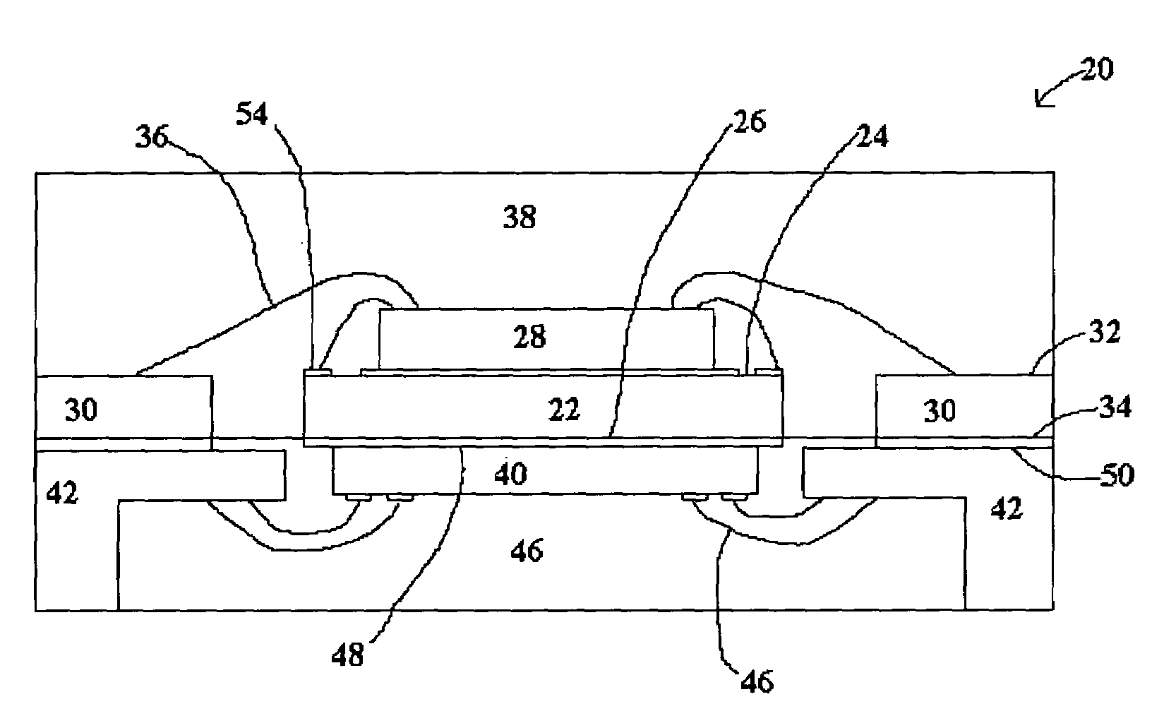
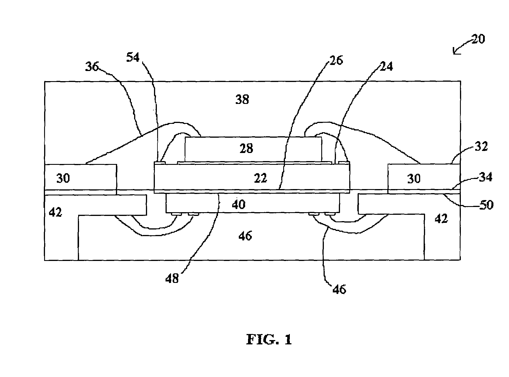
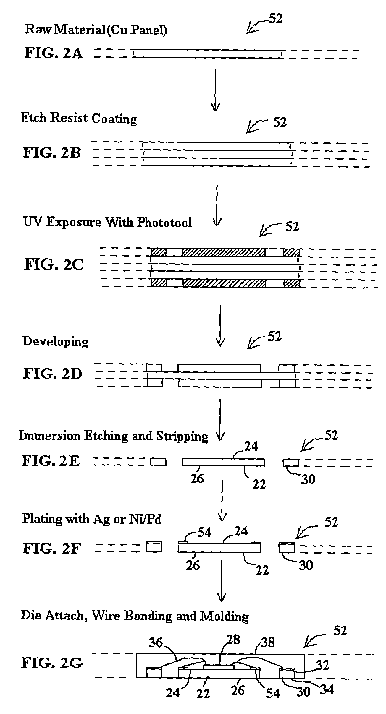
[0016]Reference is first made to FIG. 1, a sectional side view of a shielded integrated circuit package indicated generally by the numeral 20. The package 20 includes a die attach pad 22 having a first side 24 and a second side 26. A first semiconductor die 28 is mounted to the first side 24 of the die attach pad 22. A plurality of contact pads 30 are disposed in close proximity to the first semiconductor die 28 and each contact pad 30 has a first side 32 and a second side 34. A first plurality of wire bonds 36 connect the first semiconductor die 28 and ones of the contact pads 30. An overmold 38 encapsulates the first plurality of wire bonds 36 and the first semiconductor die 28. The die attach pad 22 and the contact pads 30 are embedded in the overmold 38 such that the first side 24 of the die attach pad 22 and the first side 32 of each of the contact pads 30 are encapsulated in the overmold 38. A second semiconductor die 40 is mounted to the second side 26 of the die attach pad 2...


PUM


Abstract

An integrated circuit package is provided. The package includes a die attach pad having a first side and a second side. A first semiconductor die is mounted to the first side of the die attach pad, a plurality of contact pads disposed in close proximity to the first semiconductor die. A first plurality of wire bonds connect the first semiconductor die and ones of the contact pads. An overmold encapsulates the first plurality of wire bonds and the first semiconductor die, the die attach pad and the contact pads being embedded in the overmold. A plurality of leads are disposed proximal the second side of the die attach pad. A second semiconductor die is mounted to one of the second side of the die attach pad and ones of the plurality of leads such that the ones of the plurality of leads are electrically connected to the second semiconductor die. The second semiconductor die and the leads are embedded in an encapsulant. The die attach pad shields the second semiconductor die.

Description

FIELD OF THE INVENTION[0001]The present invention relates in general to integrated circuit packaging, and more particularly to an integrated circuit package with unique radio frequency and electromagnetic interference shielding.BACKGROUND OF THE INVENTION[0002]According to well known prior art IC (integrated circuit) packaging methodologies, semiconductor dice are singulated and mounted using epoxy or other conventional means onto respective die attach pads (attach paddles) of a leadframe strip. Traditional QFP (Quad Flat Pack) packages incorporate inner leads which function as lands for wire bonding the semiconductor die bond pads. These inner leads typically require mold locking features to ensure proper positioning of the leadframe strip during subsequent molding to encapsulate the package. The inner leads terminate in outer leads that are bent down to contact a motherboard.[0003]Conventional molding materials are plastic and serve to encapsulate, protect and provide support for ...

Claims


Application Information

Patent Timeline
Patent Type & Authority Patents(United States)
IPC IPC(8): H01L23/02
CPCH01L23/3135H01L23/49537H01L23/552H01L23/49575H01L2224/45144H01L2224/73265H01L2224/32245H01L2224/48257H01L2224/16245H01L24/48H01L2924/3025H01L2924/1532H01L2924/01079H01L2924/01078H01L2224/48091H01L2224/48247H01L2924/01046H01L2924/00014H01L2924/00012H01L2924/00H01L24/45H01L24/73H01L2924/14H01L2924/181
Inventor PATEL, VIRESHKIRLOSKAR, MOHAN
Owner UTAC HEADQUARTERS PTE LTD
Why Eureka
Try Eureka