High speed, high density electrical connector

a high density, electrical connector technology, applied in the direction of coupling device connection, connection contact member material, coupling protective earth/shielding arrangement, etc., can solve the problem of a large possibility of electrical noise being generated in the connector, a significant limitation on single-ended signal use of the system, and a large number of electrical noise generation

Inactive Publication Date: 2006-07-11
AMPHENOL CORP
View PDF55 Cites 147 Cited by
  • Summary
  • Abstract
  • Description
  • Claims
  • Application Information

AI Technical Summary

Problems solved by technology

Electronic systems have generally become smaller, faster and functionally more complex.
As signal frequencies increase, there is a greater possibility of electrical noise being generated in the connector in forms such as reflections, cross-talk and electromagnetic radiation.
It has thus been recognized that this presents a significant limitation on single-ended signal use for systems with growing numbers of higher frequency signal paths.
While presently available differential pair electrical connector designs provide generally satisfactory performance, the inventors of the present invention have noted that at high speeds, the available electrical connector designs may not sufficiently provide desired minimal cross-talk, impedance and attenuation mismatch characteristics.
And the signal transmission characteristics degrade.
These problems are more significant when the electrical connector utilizes single-ended signals, rather than differential signals.

Method used


Image

  • High speed, high density electrical connector
  • High speed, high density electrical connector
  • High speed, high density electrical connector

Examples


Embodiment Construction

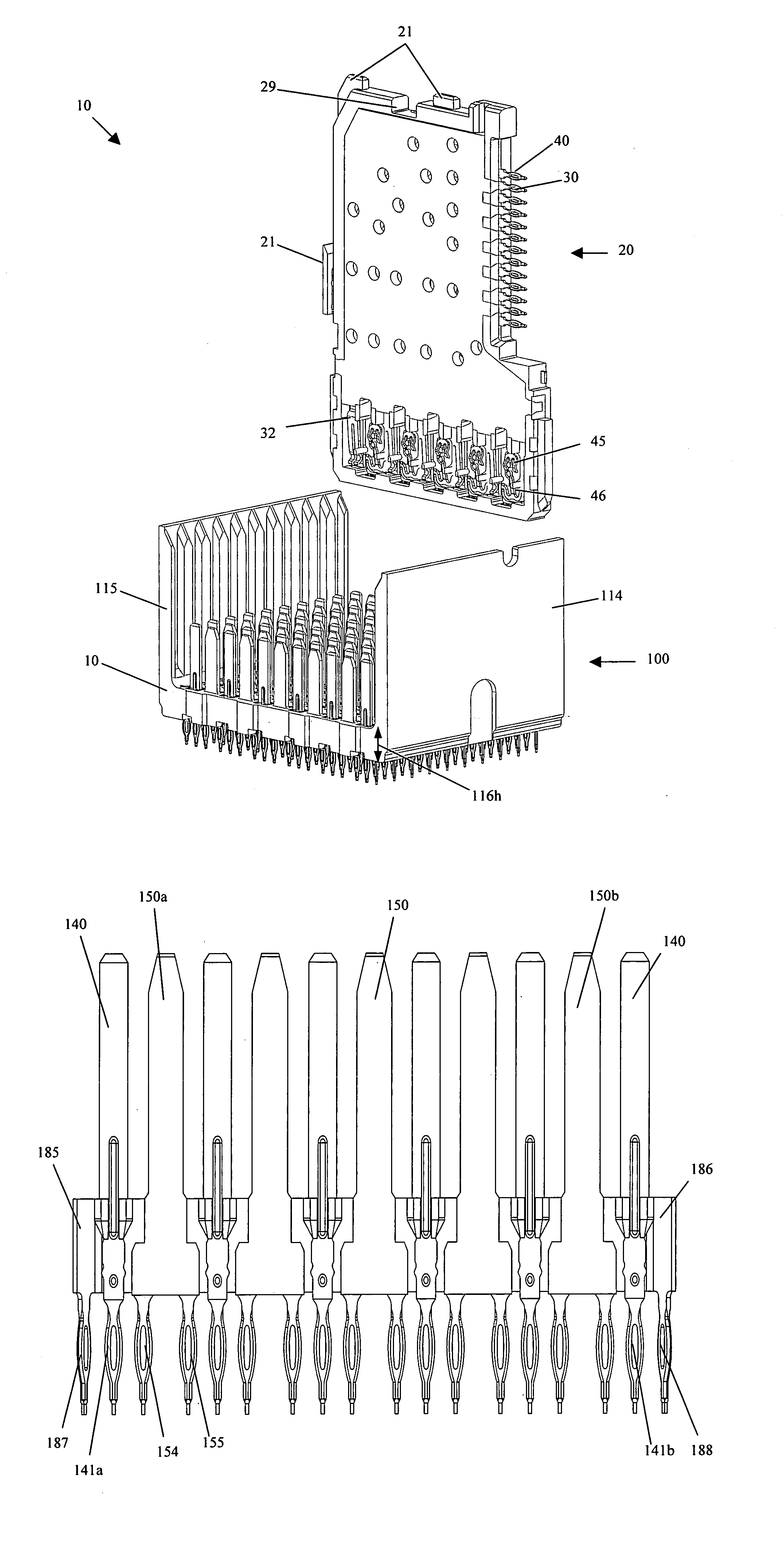
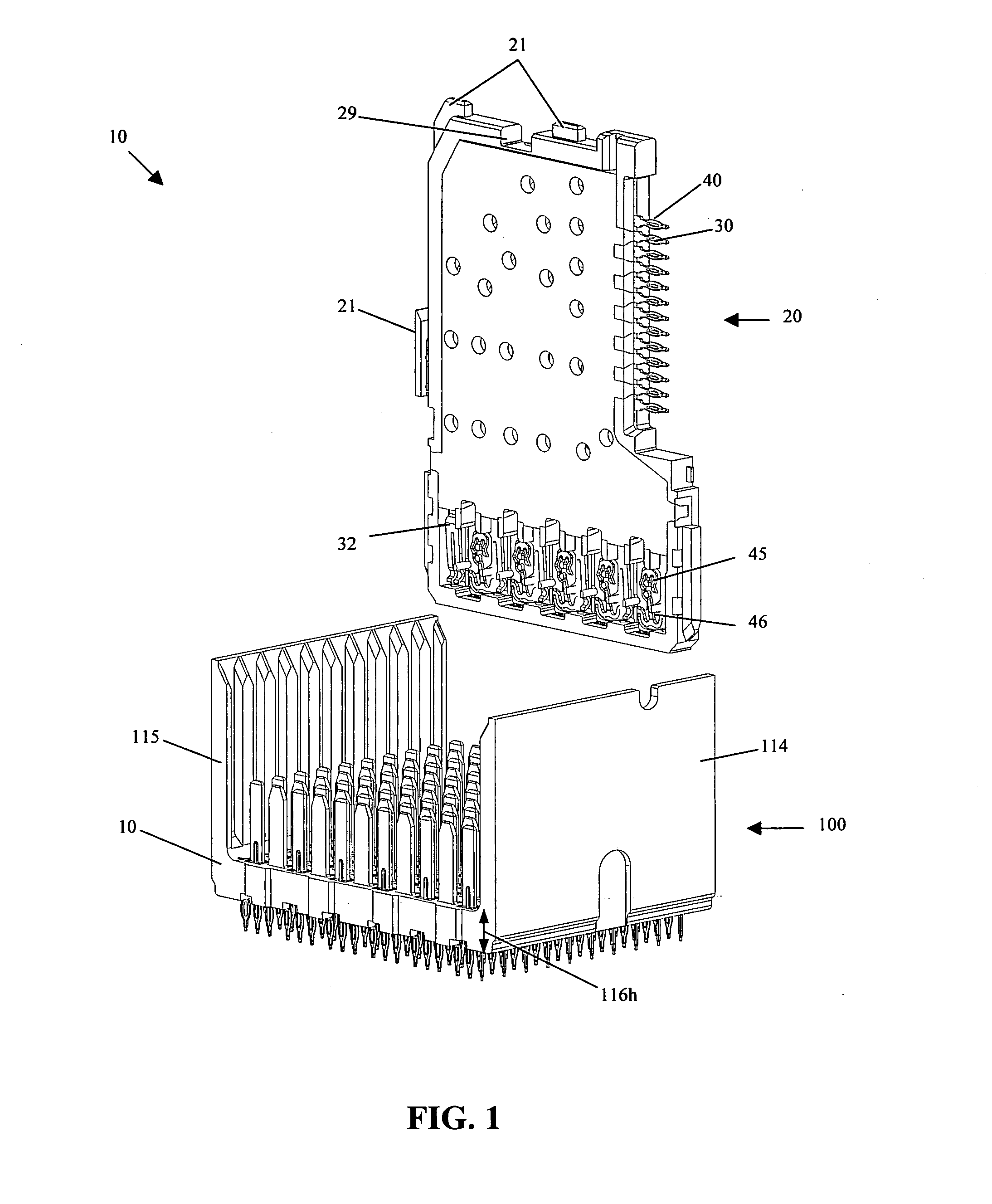
[0025]Referring to FIG. 1, there is shown an electrical connector assembly in accordance with an embodiment of the present invention. The electrical connector assembly 10 includes a first electrical connector mateable to a second electrical connector 100. The first electrical connector includes a plurality of wafers 20, only one of which is shown in FIG. 1, with the plurality of wafers 20 preferably held together by a stiffener (such as a stiffener 210 illustrated in FIG. 10). Note that each of the wafers 20 is provided with an attachment feature 21 for engaging the stiffener. For exemplary purposes only, the first electrical connector has ten wafers 20, with each wafer 20 having six single-ended signal conductors 24 and a corresponding shield plate 26 (see FIG. 2). However, as it will become apparent later, the number of wafers, the number of signal conductors and the number of shield plates may be varied as desired.

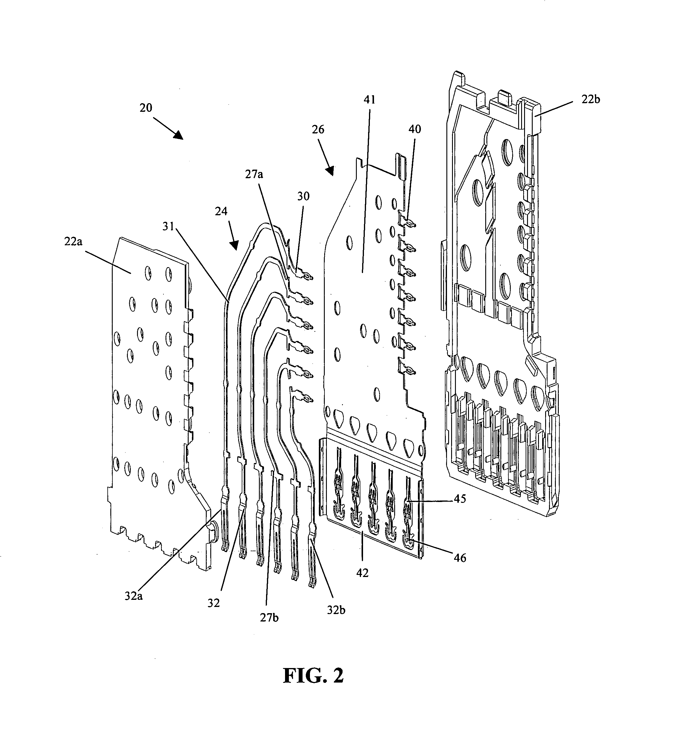
[0026]FIG. 2 is an exploded view of the wafer 20 of FIG. 1. The wa...


PUM


Abstract

In one embodiment of the invention, there is disclosed an electrical connector connectable to a printed circuit board, the electrical connector having an insulative housing including side walls and a base. The electrical connector also includes signal conductors and ground conductors. Each of the signal conductors and ground conductors has a first contact end connectable to the printed circuit board, a second contact end, and an intermediate portion therebetween that is disposed in the base of the insulative housing. The signal conductors and the ground conductors are arranged in a plurality of rows, with each row having signal conductors and ground conductors. For each of the plurality of rows, there is a corresponding ground strip positioned adjacent thereto disposed in the base of the insulative housing. And the ground strip is electrically connected to the ground conductors of the row.

Description

BACKGROUND OF THE INVENTION[0001]This invention relates generally to an electrical connector assembly for interconnecting printed circuit boards. More specifically, this invention relates to a high speed, high density electrical connector and connector assembly.[0002]Electrical connectors are used in many electronic systems. It is generally easier and more cost effective to manufacture a system on several printed circuit boards (“PCBs”) which are then connected to one another by electrical connectors. A traditional arrangement for connecting several PCBs is to have one PCB serve as a backplane. Other PCBs, which are called daughter boards or daughter cards, are then connected through the backplane by electrical connectors.[0003]Electronic systems have generally become smaller, faster and functionally more complex. This typically means that the number of circuits in a given area of an electronic system, along with the frequencies at which the circuits operate, have increased signific...

Claims


Application Information

Patent Timeline
Patent Type & Authority Patents(United States)
IPC IPC(8): H01R13/58H01R12/16
CPCH01R23/688H01R12/585H01R13/6585H01R12/00
Inventor COHEN, THOMAS S.CARTIER, MARC B.DUNHAM, JOHN R.PAYNE, JASON J.
Owner AMPHENOL CORP
Why Eureka
Try Eureka