Binary half tone photomasks and microscopic three-dimensional devices and method of fabricating the same

a three-dimensional device and photomask technology, applied in the direction of photomechanical equipment, relative volume flow measurement, instruments, etc., can solve the problems of inability to meet production requirements in a cost-effective manner, inability to use micro-machining tools, and inability to work well with commonly applied techniques for manufacturing integrated circuits

Inactive Publication Date: 2006-07-11
PHOTRONICS INC
View PDF19 Cites 13 Cited by
  • Summary
  • Abstract
  • Description
  • Claims
  • Application Information

AI Technical Summary

Problems solved by technology

However, this method was time consuming and expensive, and thus, it was typically difficult for manufacturers to meet production requirements in a cost efficient manner.
In this regard, such techniques did not work well with commonly applied techniques for manufacturing integrated circuits because each pixel of the design had to be rewritten using a new algorithm.
Since this was a laborious and time-consuming undertaking, many have avoided the use of micro-machining tools.
As a practical matter, however, the k factor can be somewhat greater than 0.5 and still be unresolved by the total process for some exposure tools.
Unfortunately, there are many other tools which do not meet the requirements of equation (1), and thus, the design of the photomask is often limited by the capabilities of the design tools available to the designer.
Moreover, since photomasks are commonly designed to include other structures (e.g., two dimensional, binary components such as integrated circuit patterns) in addition to a three-dimensional device (e.g., photonics application), this problem is even more complex than implied by the above equation.
In some applications where the specifications of the device permit, a ripple-effect may be acceptable, albeit undesirable.
However, in many applications, a sub-ripple effect is not acceptable since a smoother profile is needed for optimal performance of the device being fabricated.
Since the prior art BHT photomask design requires the use of a small k factor to achieve a smoother profile, the mask designer is limited to equipment meeting this requirement.
As a result, the mask designer is limited to only those write tools that have the ability to match the gray level grid design associated therewith.
For example, an electron beam write tool such as the MEBES 4500, with a write grid of 20 nm cannot properly replicate a BHT design whose sub-pixel variations is 10 nm.
Moreover, an imaging solution requiring custom materials at the mask will often add cost and complexity in the overall manufacturing process due to the difficulties typically associated with integrating new materials into a photomask.
However, VAFs are typically expensive and yield less than desirable results.
It is noted, however, that the photoresist process is often limited to the variable dose pattern generator being used.
These methods, however, have their limitations.
In this regard, it is known that contact hole and spot features are more difficult to control than line and space features.
As a result, both corner rounding and linearity of the design are compromised.
Similarly, variable pitch methods are problematic since they require a different algorithm to be applied at each pixel position to carefully define the correct opening in the BHT mask.
This can limit the ability of a mask designer to make the fine changes required to correct for process non-linearity.
These methods add to the costs and processing time in preparation of the mask since they require a large number of adjustments to be made to the overall design.
As a result, the change in area of each sub-pixel is a square of the amplitude, thereby making the change in light intensity between each gray level non-linear and often infinite.
Accordingly, three-dimensional objects made by the prior art methods tend to have jagged surfaces, especially where the objects are sloped.
Since these methods produce marginal results, many have migrated away from the use of BHT photomasks for making three-dimensional microscopic devices.

Method used


Image

  • Binary half tone photomasks and microscopic three-dimensional devices and method of fabricating the same
  • Binary half tone photomasks and microscopic three-dimensional devices and method of fabricating the same
  • Binary half tone photomasks and microscopic three-dimensional devices and method of fabricating the same

Examples


Embodiment Construction

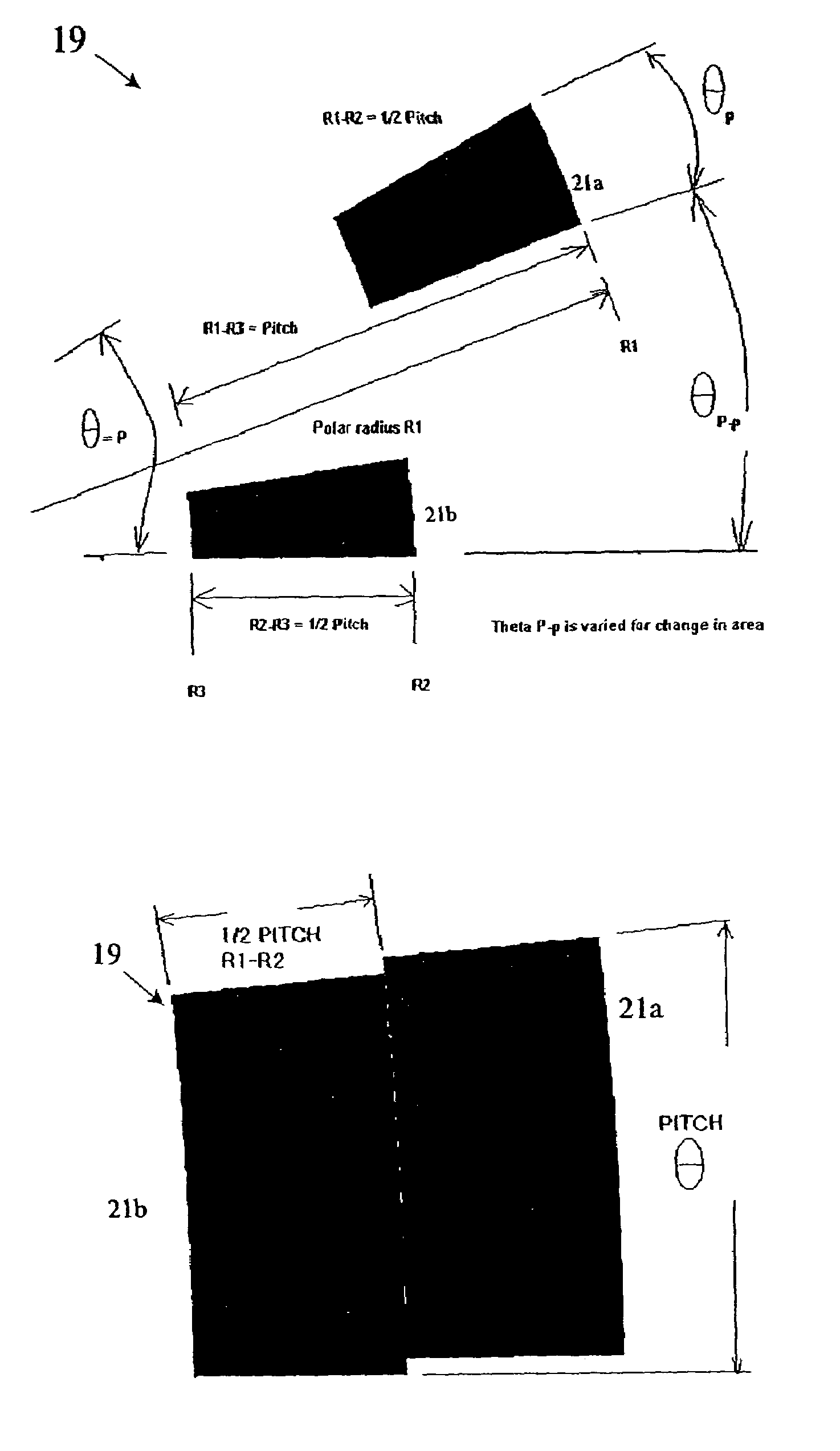
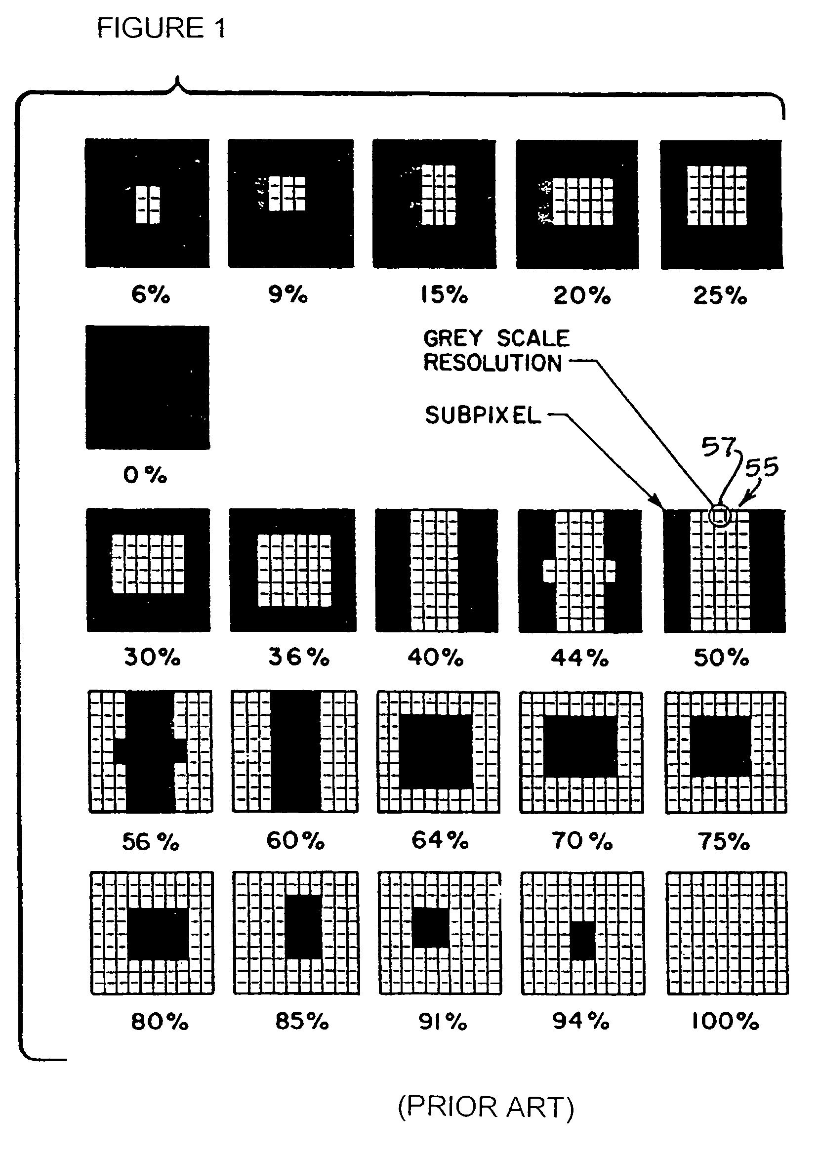
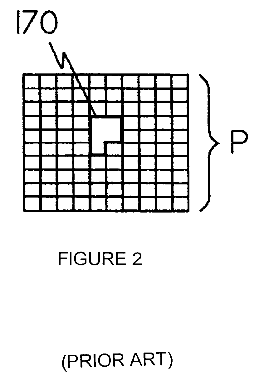
[0047]The present invention generally relates to improved BHT photomasks and microscopic three-dimensional structures made from such photomasks. The present invention is also directed toward a method for designing and fabricating BHT photomasks to be used in creating such microscopic three-dimensional structures (e.g., MEMS, micro-optics, photonics, micro-structures and other three-dimensional, microscopic devices). More particularly, the present provides a method for designing a BHT photomask layout, transferring the layout to a BHT photomask and fabricating three-dimensional microscopic structures using the BHT photomask designed by the method of the present invention. As will be seen below, the method of the present invention enables a photomask designer to design a BHT photomask to have continuous gray levels such that the change in light intensity between each gray level is both finite and linear. As a result, when this BHT photomask is used to make a three-dimensional microsco...


PUM

PropertyMeasurementUnit
sizesaaaaaaaaaa
sizeaaaaaaaaaa
sizeaaaaaaaaaa

Abstract

The present invention generally relates to improved binary half tone (“BHT”) photomasks and microscopic three-dimensional structures (e.g., MEMS, micro-optics, photonics, micro-structures and other three-dimensional, microscopic devices) made from such BHT photomasks. More particularly, the present invention provides a method for designing a BHT photomask layout, transferring the layout to a BHT photomask and fabricating three-dimensional microscopic structures using the BHT photomask designed by the method of the present invention. In this regard, the method of designing a BHT photomask layout comprises the steps of generating at least two pixels, dividing each of the pixels into sub-pixels having a variable length in a first axis and fixed length in a second axis, and arraying the pixels to form a pattern for transmitting light through the pixels so as to form a continuous tone, aerial light image. The sub-pixels' area should be smaller than the minimum resolution of an optical system of an exposure tool with which the binary half tone photomask is intended to be used. By using this method, it is possible to design a BHT photomask to have continuous gray levels such that the change in light intensity between each gray level is both finite and linear. As a result, when this BHT photomask is used to make a three-dimensional microscopic structure, it is possible to produce a smoother and more linear profile on the object being made.

Description

RELATED APPLICATIONS[0001]This application is a divisional of U.S. patent application Ser. No. 10 / 349,629, filed Jan. 23, 2003 now U.S. Pat. No. 6,828,068.FIELD OF THE INVENTION[0002]The present invention generally relates to binary half tone (“BHT”) photomasks and three-dimensional microscopic structures (e.g., micro-electromechanical systems (“MEMS”), micro-optics, photonics, micro-structures, imprint lithography applications and other devices) and a method for designing and fabricating the same.BACKGROUND OF THE INVENTION[0003]Recent technological advances have made it possible to use three-dimensional MEMS, micro-optical devices and other micro-structures in a variety of fields, including photonics, communications, and integrated circuits. In the past, these tiny devices were fabricated using laser micro-machining tools. However, this method was time consuming and expensive, and thus, it was typically difficult for manufacturers to meet production requirements in a cost efficien...

Claims


Application Information

Patent Timeline
Patent Type & Authority Patents(United States)
IPC IPC(8): G01F9/00G03C5/00G03F1/00G03F7/00G03F9/00G06F17/50G06K15/00H01LH01L21/027H04N1/405
CPCB82Y10/00B82Y40/00G03F7/0005G03F1/144G03F1/14G03F7/0002G03F1/50G03F1/62G03F1/38G03F9/00G03C5/00
Inventor PROGLER, CHRISTOPHER J.RHYINS, PETER
Owner PHOTRONICS INC
Why Eureka
Try Eureka