Superconducting system, superconducting circuit chip, and high-temperature superconducting junction device with a shunt resistor

a superconducting circuit and superconducting circuit technology, applied in the direction of superconductor devices, semiconductor devices, electrical appliances, etc., can solve the problems of insufficient performance of the nb latch interface circuit, inability to drive the semiconductor device directly, and significant increase in hysteresis, so as to achieve sufficient amplification capability

Inactive Publication Date: 2006-07-11
FUJITSU LTD +1
View PDF1 Cites 19 Cited by
  • Summary
  • Abstract
  • Description
  • Claims
  • Application Information

AI Technical Summary

Benefits of technology

[0023]The present invention was made under the background circumstances described above. An object of the present invention is to provide a superconducting system including an interface circuit which can transmit a signal outputted from a superconducting circuit to another circuit at a high speed, which has sufficient amplification capability, and which hardly malfunctions.

Problems solved by technology

However, this SFQ circuit operates at a voltage of about several hundred microvolts, so it cannot drive the semiconductor device directly.
As described above, the performance of the Nb latch interface circuit is not yet adequate enough to serve as an interface circuit between the Nb superconducting circuit and a semiconductor circuit.
According to a further study by the present inventor, however, an increase in the critical current density Jc leads to a significant increase in the hysteresis.
Such an increase in the hysteresis tends to decrease a bias margin for the SFQ circuit.
When the hysteresis exceeds 10%, it is difficult for the SFQ circuit to operate.
If the SFQ circuit is complex, it cannot operate.
That is to say, an increase in the critical current density Jc leads to a steep increase in the hysteresis.

Method used


Image

  • Superconducting system, superconducting circuit chip, and high-temperature superconducting junction device with a shunt resistor
  • Superconducting system, superconducting circuit chip, and high-temperature superconducting junction device with a shunt resistor
  • Superconducting system, superconducting circuit chip, and high-temperature superconducting junction device with a shunt resistor

Examples


first embodiment

[0052]The first embodiment will be described first.

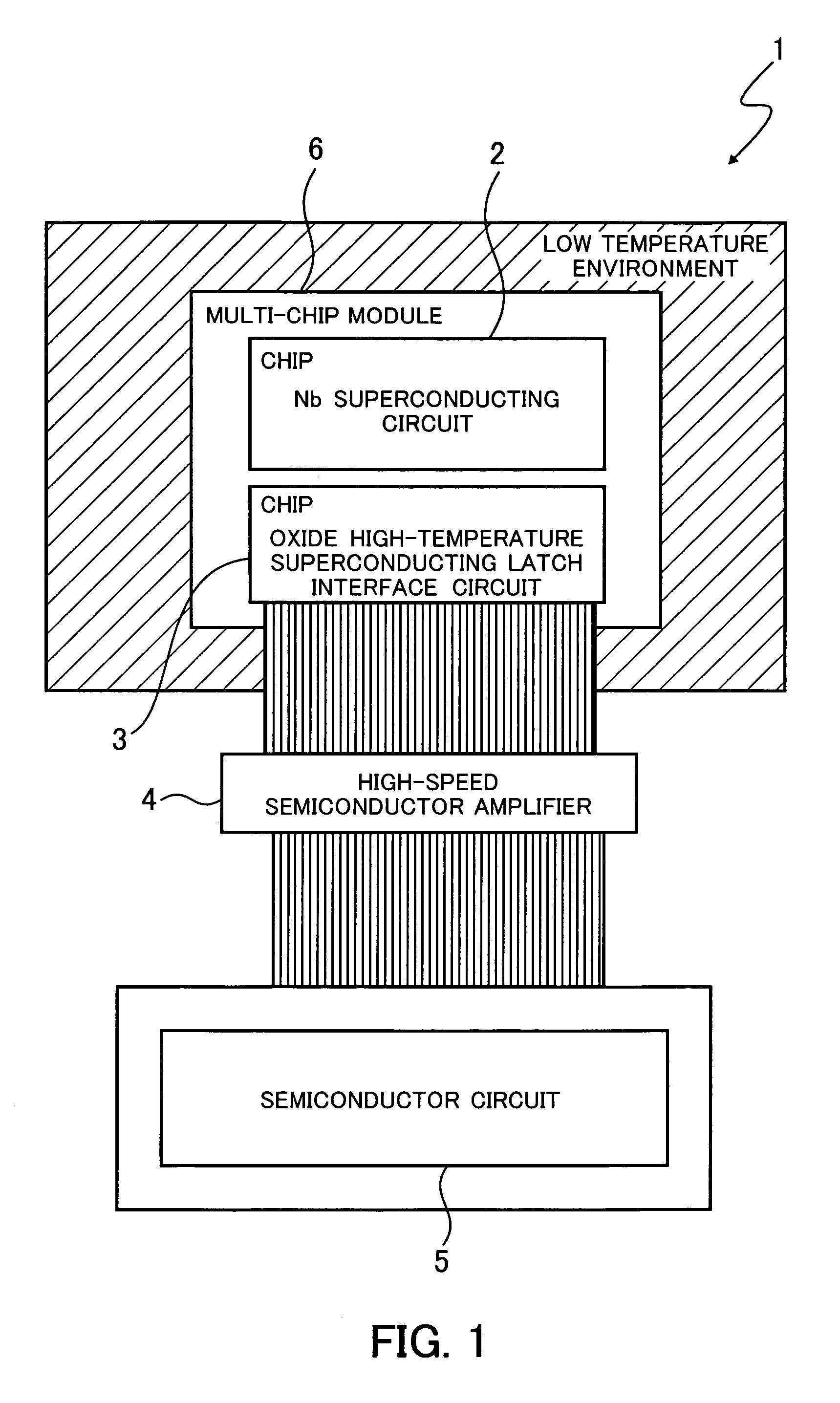
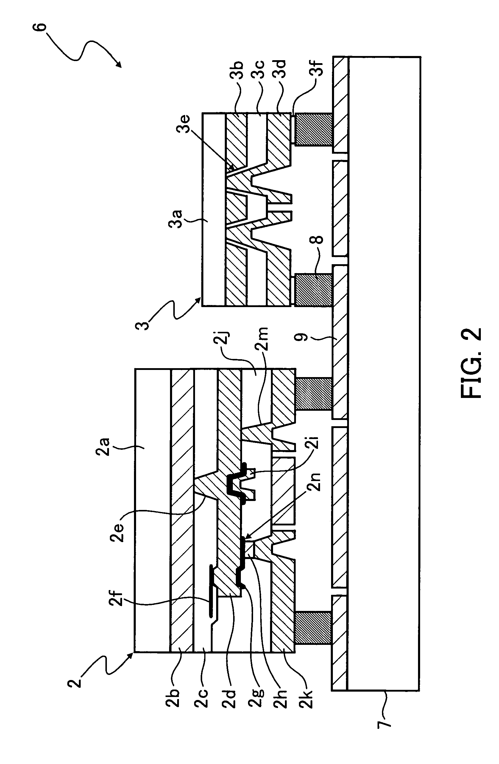
[0053]FIG. 1 shows the structure of a superconducting system according to the first embodiment of the present invention. A superconducting system 1 shown in FIG. 1 comprises an Nb superconducting circuit 2, being a low-temperature superconducting circuit formed by the use of Nb, and an oxide high-temperature superconducting latch interface circuit 3, being a latch driver formed by the use of an oxide high-temperature superconductor. The Nb superconducting circuit 2 is an SFQ circuit having a Josephson junction formed by the use of Nb. The oxide high-temperature superconducting latch interface circuit 3 is an interface circuit having a Josephson junction formed by the use of an oxide high-temperature superconductor having composition, such as YBaCuO, YbBaCuO, DyBaCuO, ErBaCuO, HoBaCuO, or NdBaCuO. The Nb superconducting circuit 2 and the oxide high-temperature superconducting latch interface circuit 3 are in a low temperature environ...

second embodiment

[0067]The second embodiment will now be described.

[0068]FIG. 3 shows the structure of a superconducting system according to the second embodiment of the present invention. Components in FIG. 3 which are the same as those shown in FIG. 1 are marked with the same symbols and detailed descriptions of them will be omitted.

[0069]A superconducting system 20 according to the second embodiment of the present invention differs from the superconducting system 1 according to the first embodiment of the present invention in that an Nb superconducting circuit 2 and an oxide high-temperature superconducting latch interface circuit 3 are formed on the same substrate, that is to say, in that there is only one superconducting circuit chip 21. The rest of the structure of the superconducting system 20 is the same as that of the superconducting system 1. In addition, the function and effect of the superconducting system 20 are the same as those of the superconducting system 1. That is to say, the chip...

third embodiment

[0071]The third embodiment will now be described.

[0072]FIG. 4 shows the structure of a superconducting system according to the third embodiment of the present invention. Components in FIG. 4 which are the same as those shown in FIG. 1 are marked with the same symbols and detailed descriptions of them will be omitted.

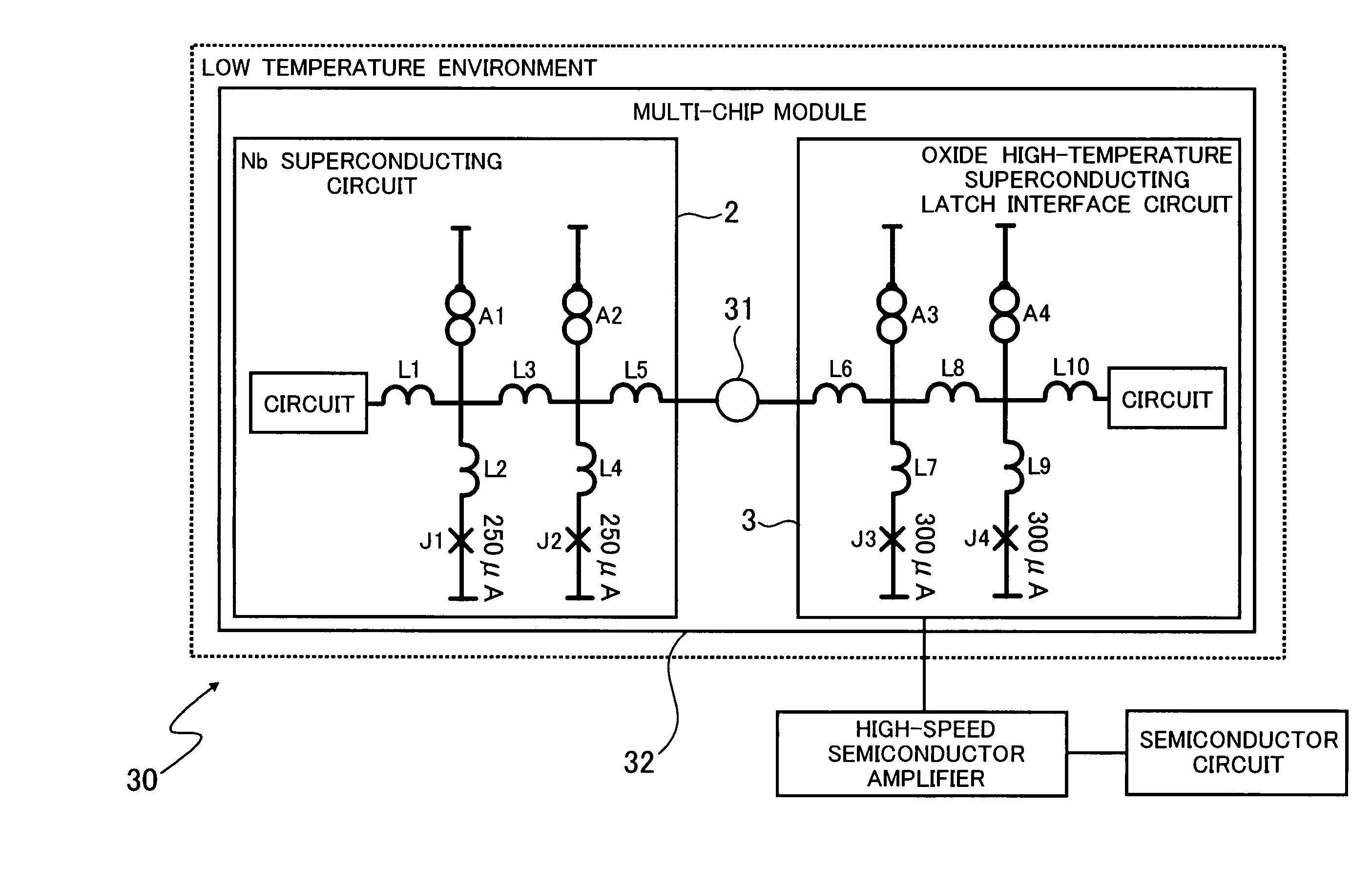
[0073]In a superconducting system 30 according to the third embodiment of the present invention, an Nb superconducting circuit 2 and an oxide high-temperature superconducting latch interface circuit 3 are not connected by a wiring, such as a PTL or a JTL. JTLs in both circuits are connected via a superconductive solder bump 31 and these circuits make up a multi-chip module 32. In the superconducting system 30, the Nb superconducting circuit 2 and the oxide high-temperature superconducting latch interface circuit 3 connected by the bump in this way are located in a low temperature environment. The rest of the structure of the superconducting system 30 is the same as that ...


PUM


Abstract

A superconducting system that includes an interface circuit capable of making the best use of a high-speed superconducting circuit and a high-speed semiconductor circuit. A multi-chip module in which an Nb superconducting circuit having josephson junctions formed by the use of Nb and an oxide high-temperature superconducting latch interface circuit having josephson junctions formed by the use of an oxide high-temperature superconductor are connected is located in a low temperature environment kept at 4.2 K. The oxide high-temperature superconducting latch interface circuit is connected to a high-speed semiconductor amplifier and a signal outputted from the Nb superconducting circuit is transmitted to the high-speed semiconductor amplifier. As a result, the limit of the operation speed of the oxide high-temperature superconducting latch interface circuit is raised and the superconducting system including the interface circuit capable of making the best use of both the high-speed Nb superconducting circuit and the high-speed semiconductor amplifier is realized.

Description

CROSS-REFERENCE TO RELATED APPLICATIONS[0001]This application is based upon and claims the benefits of priority from the prior Japanese Patent Applications No. 2003-64937, filed on Mar. 11, 2003, and No. 2003-202817, filed on Jul. 29, 2003, the entire contents of which are incorporated herein by reference.BACKGROUND OF THE INVENTION[0002](1) Field of the Invention[0003]The present invention relates to a superconducting system and a superconducting circuit chip and, more particularly, to a superconducting system for transmitting a signal outputted from a superconducting circuit to another circuit via an interface circuit and a superconducting circuit chip including such a superconducting circuit and interface circuit. Furthermore, this invention relates to a high-temperature superconducting junction device with a shunt resistor and, more particularly, to a high-temperature superconducting junction device with a shunt resistor for optimally driving a ramp-edge high-temperature superco...

Claims


Application Information

Patent Timeline
Patent Type & Authority Patents(United States)
IPC IPC(8): H01L39/00H01L27/18H01L39/22
CPCH01L39/225H01L27/18H10N69/00H10N60/124
Inventor HATO, TSUNEHIRO
Owner FUJITSU LTD
Why Eureka
Try Eureka