High-pressure processing chamber for a semiconductor wafer

a processing chamber and semiconductor technology, applied in the field of processing chambers, can solve the problems of contaminating the wafer, increasing the cost of processing system, and prone to failure of sealing components that bear the highest attainable sealing force for an unnecessary length of time, so as to maintain the sealing volume and achieve the effect of higher sealing pressur

Inactive Publication Date: 2006-07-18
TOKYO ELECTRON LTD
View PDF286 Cites 10 Cited by
  • Summary
  • Abstract
  • Description
  • Claims
  • Application Information

AI Technical Summary

Benefits of technology

[0008]In one embodiment of the present invention, the processing volume seal is maintained by a plate contained within one of the upper element and the lower element. A first face of the plate is contained within the processing volume and a second, opposing face of the plate is contained within the seal-energizing cavity. The second face has a cross-sectional area larger than a cross-sectional area of the first face. Thus when the same pressure is applied to both the first face and the second face, the force applied to the second face (the sealing force) is larger than the force applied to the first face (the processing force), maintaining the upper element against the lower element and thus maintaining the processing volume seal.
[0009]Other embodiments of the present invention comprise venting means to vent the processing volume when a processing pressure used to generate a processing force exceeds a sealing pressure used to generate a sealing force, thus aborting the device processing. This structure ensures that when the processing volume cannot be maintained, processing materials can be diverted and stored rather than dispersed to the surrounding environment.
[0010]Other embodiments of the present invention comprise a pressure intensifier, which takes a small pressure and intensifies it to produce a higher sealing pressure. The pressure intensifier thus allows the sealing pressure to be attained with a low input pressure generated within a small volume or with a low pressure relative to the processing pressure.
[0011]Other embodiments of the present invention comprise a first pressure transducer, a second pressure transducer, and an electronic controller. The first pressure transducer is coupled to the processing volume, monitors the processing pressure, and generates a related processing signal. The second pressure transducer is coupled to a low-pressure chamber used to generate the sealing pressure and thus maintain the processing volume seal. The second pressure transducer monitors the sealing pressure and generates a related sealing signal. The electronic controller receives at least one of the processing signal and the sealing signal and adjusts one of the processing pressure and the sealing pressure so that the sealing force counterbalances the processing force.

Problems solved by technology

First, sealing components that bear the highest attainable sealing force for an unnecessary length of time are prone to failure after repeated applications of the sealing force.
Second, the large contact forces on the sealing face produce particulates that are introduced into the processing volume and contaminate the wafer.
Third, the equipment used to pressurize the hydraulic fluids adds costs to the processing system, since the equipment is used to seal the processing chamber and not to process a wafer.
Fourth, those systems that could be designed to replace hydraulic components with supercritical components using supercritical processing materials are expensive.
These systems require complicated recycling techniques because the supercritical processing materials must be expanded and pressurized before they can be reused.

Method used


Image

  • High-pressure processing chamber for a semiconductor wafer
  • High-pressure processing chamber for a semiconductor wafer
  • High-pressure processing chamber for a semiconductor wafer

Examples


Embodiment Construction

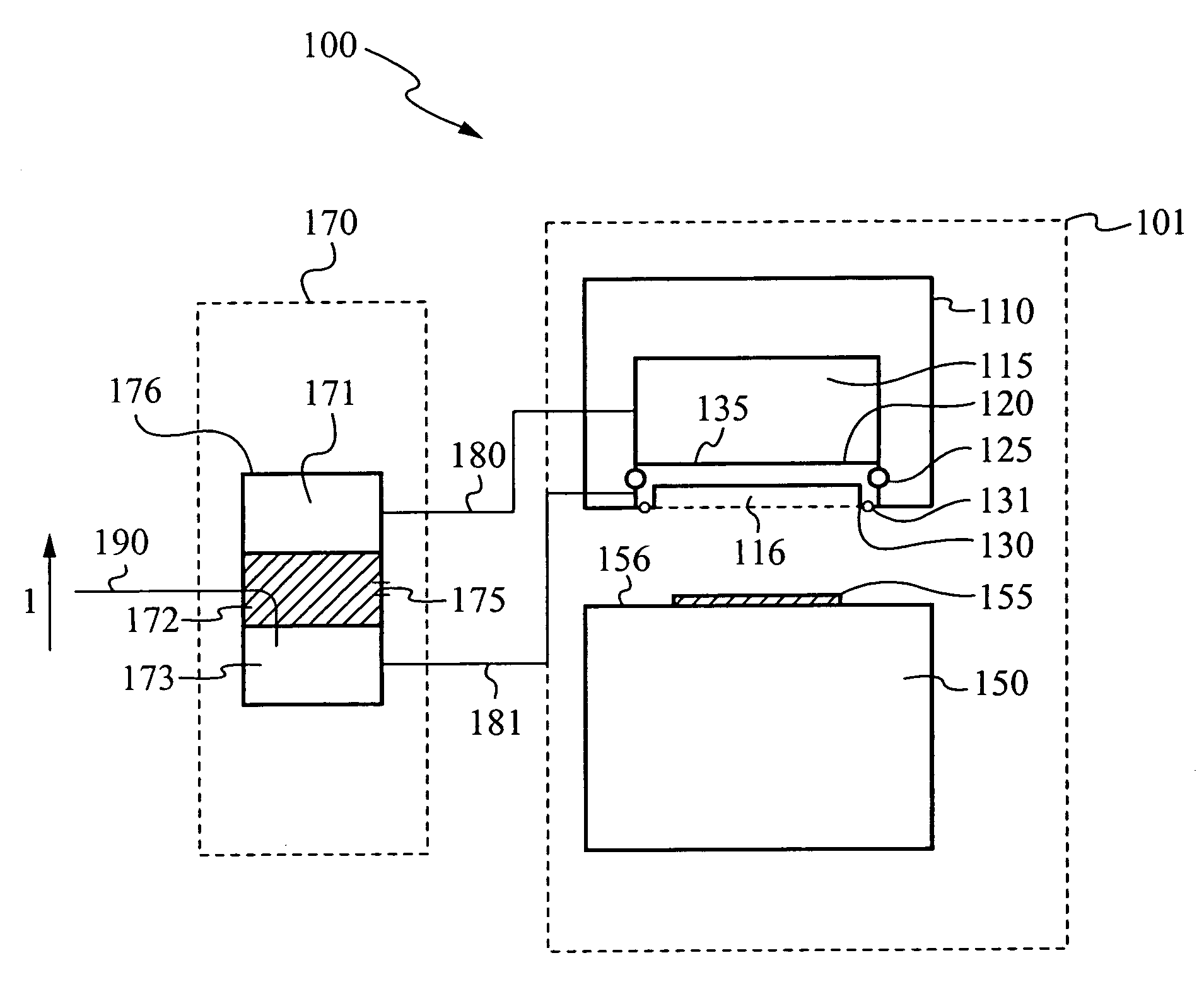
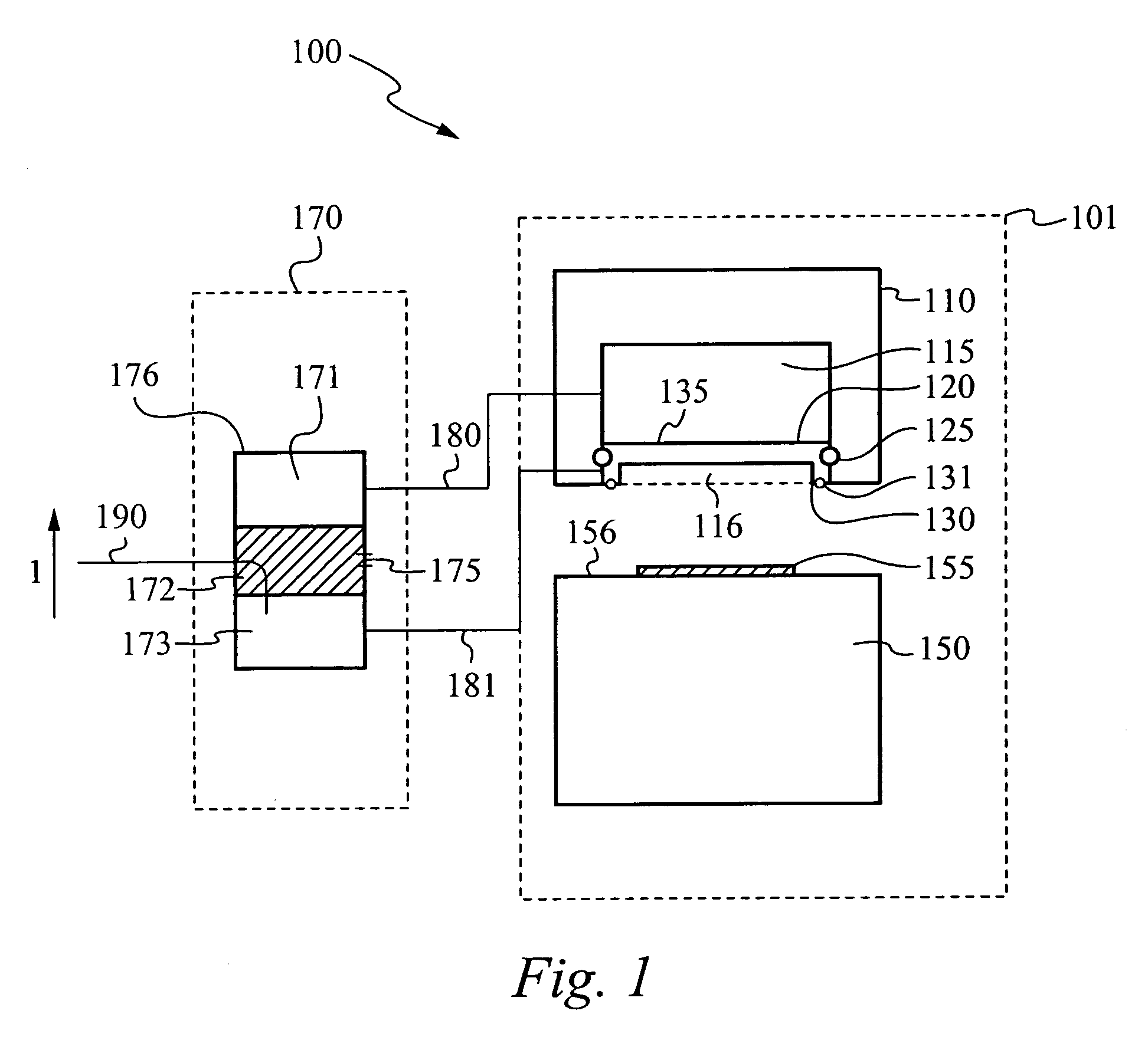
[0023]The present invention is directed to a system for and method of efficiently maintaining a processing volume during device processing. When a semiconductor wafer undergoes processing in a processing chamber, it is subjected to a range of processing temperatures and pressures. For the processing to be performed correctly-that is, for a semiconductor wafer to be processed without being exposed to contaminants-the processing volume must remain hermetically sealed during processing. Moreover, the processing volume should remain sealed using the minimum force necessary.

[0024]As used herein, processing pressure refers to the pressure generated within a processing volume during device processing, and accordingly may vary during device processing. Processing force refers to the force generated by the processing pressure and exerted against a face of the processing volume. Sealing pressure refers to the pressure generated within a seal-energizing cavity (described below). Sealing force ...


PUM


Abstract

A processing chamber having an improved sealing means is disclosed. The processing chamber comprises a lower element, an upper element, and a sealing means that tightly holds the lower element to the upper element to define a processing volume that is maintained using the minimum pressure necessary. The processing chamber comprises a plate having a first face that forms the processing volume and a second, opposing face that forms a seal-energizing cavity. In one embodiment, a surface area of the first face is smaller than a surface area of the second face. When the same pressure is applied against both the first face and the second face, the force on the second face is greater than the force on the first face, resulting in a sealing force exceeding a processing force generated within the processing volume.

Description

FIELD OF THE INVENTION[0001]This invention relates to the field of processing chambers. More particularly, this invention relates to a system and a method for reliably sealing a high-pressure processing chamber.BACKGROUND OF THE INVENTION[0002]A semiconductor device is fabricated by placing it in a processing chamber in which device layers are formed, processing residue is removed, and other processing steps are performed on it. In addition, certain processing chambers are used for cleaning semiconductor wafers at supercritical temperatures and pressures.[0003]Generally, processing chambers contain an upper element and a lower element. When the two elements are brought together, they form a processing volume in which a wafer is contained during processing. During processing, it is critical that the processing volume remain sealed so that it can be maintained at correct operating conditions, such as high-pressure, atmospheric, or supercritical conditions. Sealing the processing volum...

Claims


Application Information

Patent Timeline
Patent Type & Authority Patents(United States)
IPC IPC(8): B08B3/02H01L21/00
CPCH01L21/67126Y10S134/902
Inventor JONES, WILLIAM DALE
Owner TOKYO ELECTRON LTD
Why Eureka
Try Eureka