Substrate fabrication method and substrate

Active Publication Date: 2006-07-18
SHINKO ELECTRIC IND CO LTD
View PDF6 Cites 33 Cited by
  • Summary
  • Abstract
  • Description
  • Claims
  • Application Information

AI Technical Summary

Benefits of technology

[0010]It is a general object of the present invention to provide a substrate fabri

Problems solved by technology

As a result, Cu powder may arise from the Cu conductive parts 4 through the back-grinding, resulting in clogging the grindstone surface.
Thus, there occurs a problem of complicating grin

Method used


Image

  • Substrate fabrication method and substrate
  • Substrate fabrication method and substrate
  • Substrate fabrication method and substrate

Examples


Embodiment Construction

[0034]In the following, embodiments of the present invention will be described with reference to the accompanying drawings.

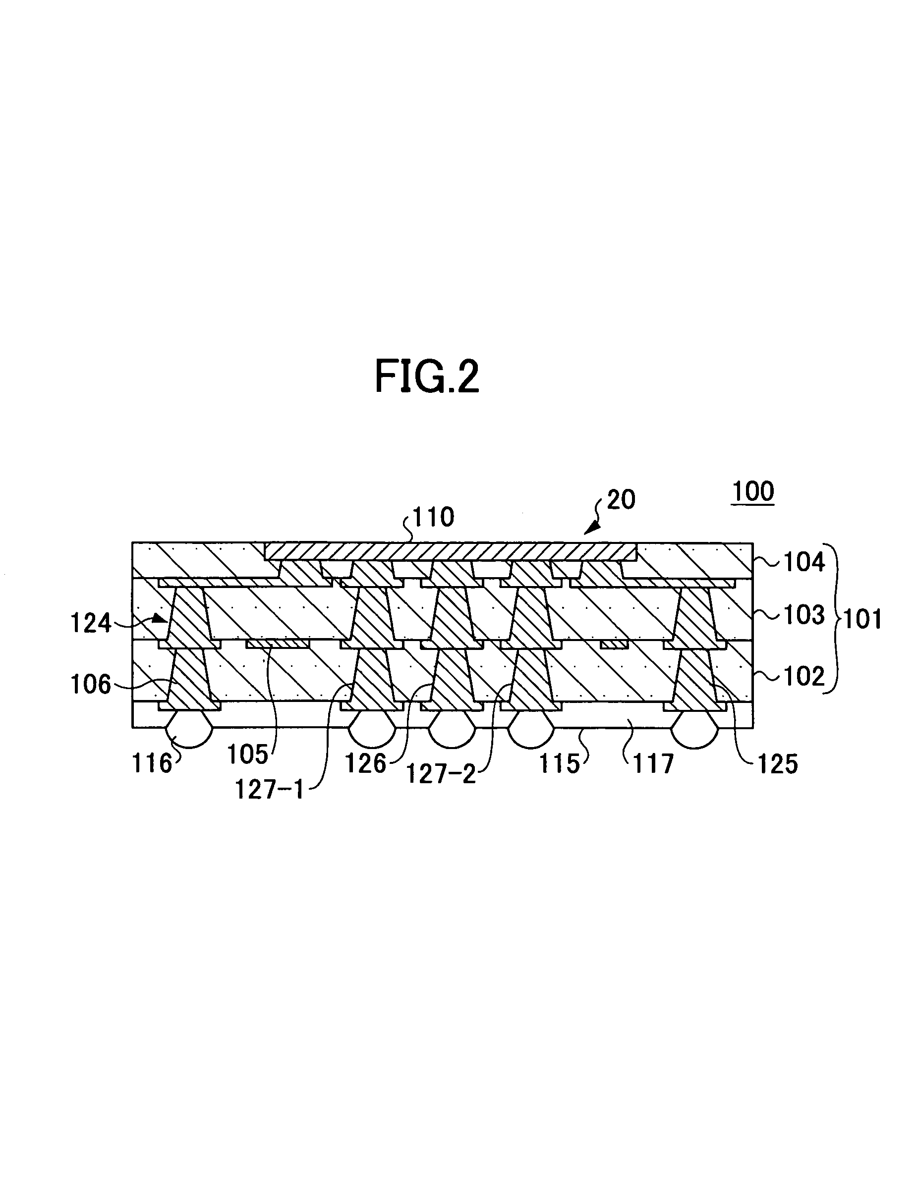
[0035]FIG. 2 is a cross-sectional view of a semiconductor device substrate 100 according to an embodiment of the present invention. FIG. 3A is an enlarged view of a portion of the semiconductor device substrate 100 shown in FIG. 2. FIGS. 3B and 3C are cross-sectional views of the semiconductor device substrate 100 with respect to the BB plane and the CC plane, respectively, illustrated in FIG. 3A.

[0036]Referring to FIG. 2, the semiconductor device substrate 100 comprises a substrate body 101 and a capacitor element 20 embedded in the upper surface of the substrate body 101. On the semiconductor device substrate 100, a LSI semiconductor element 140 is mounted as illustrated in FIG. 3 and FIG. 5 described in detail below. A semiconductor device 130 shown in FIG. 5 is often mounted on a print substrate of an electronic device.

[0037]It is noted that substantial part...


PUM


Abstract

An efficient substrate fabrication method is disclosed. A method of fabricating a substrate having a via terminal includes the steps of: forming a concave part on a front surface of a source substrate; forming a front surface side conductive part by filling the concave part with a conductor; forming the core substrate by back-grinding up to a position immediately before the front surface side conductive part is exposed such that a tip of the front surface side conductive part is covered with a portion of the core substrate; exposing the tip of the front surface side conductive part by forming a concave part in a rear surface of the core substrate; forming a rear surface side conductive part by filling the concave part with a conductor; and electrically and mechanically connecting the front surface side conductive part with the rear surface side conductive part.

Description

BACKGROUND OF THE INVENTION[0001]1. Field of the Invention[0002]The present invention relates to a substrate fabrication method and a substrate.[0003]2. Description of the Related Art[0004]Recently, semiconductor devices tend to include semiconductor elements of which operating frequencies are higher. As a result, there is a stronger demand of stabilizing source voltages supplied to such semiconductor elements. For such a semiconductor device having semiconductor elements operating at high frequencies, a variety of substrate structures having embedded capacitor elements have been presented as disclosed in Japanese Laid-Open Patent Applications No. 2002-008942 and No. 2001-053218.[0005]In an exemplary presented substrate structure, a capacitor element includes a capacitor part on a silicon substrate and a via terminal to pierce the silicon substrate.[0006]FIG. 1A through 1D are diagrams to explain conventional steps of fabricating such a capacitor element.[0007]A capacitor element 1 ...

Claims


Application Information

Patent Timeline
IPC IPC(8): H01L21/58H01L23/12H01L21/48H01L21/68H01L21/768H01L23/14H01L23/15H01L23/485H01L23/498H01L23/50
CPCH01L21/4857H01L21/486H01L21/6835H01L21/76898H01L23/147H01L23/49816H01L23/49827H01L23/49833H01L23/49838H01L23/50H01L24/10H01L2221/68345H01L2221/68377H01L2224/16H01L2924/00014H01L2924/01078H01L2924/01079H01L2924/09701H01L2924/12042H01L2924/15174H01L2924/15311H01L2924/19041H01L2924/19103H01L2924/00H01L2224/0401
Inventor YAMASAKI, TOMOOROKUGAWA, AKIO
Owner SHINKO ELECTRIC IND CO LTD
Why Eureka
Try Eureka