Wiring structure, method of manufacturing the same, electro-optical device, and electronic device

Active Publication Date: 2006-07-18
138 EAST LCD ADVANCEMENTS LTD
View PDF12 Cites 4 Cited by
  • Summary
  • Abstract
  • Description
  • Claims
  • Application Information

AI Technical Summary

Benefits of technology

[0017]As described above, according to the present invention, the electrical connection between the first conductive layer and the conductive layer can be well established, while an undesired defect (for example, the piercing in the first conductive layer as described above) is drastically reduced, thereby allowing a wiring structure capable of operating excellently to be provided.
[0062]According to this aspect, since the fixed-potential-side capacitor electrode is formed so as to cover the pixel voltage side capacitor electrode, it is possible that the dielectric film is inserted into further wide area of the electrodes, thereby constructing a storage capacitor having a larger size of capacity value. In particular, for example, in the present aspect, the sidewalls of the three elements can be utilized as a capacitor, thereby expecting the increase of the capacity value. Further, from the viewpoint of this, for example, if the pixel-potential-side capacitor electrode is formed thick, the area of the sidewall becomes larger, thereby effectively obtaining the capacity value.

Problems solved by technology

However, in such electro-optical device, in general, it is not easy to construct an optimum laminated structure by optimally arranging the various elements as described above three-dimensionally.
However, it can be very difficult to form such storage capacitors on the substrate as a part of the laminated structure.
First, if the storage capacitors are merely enlarged in a plane, this reduces the pixel aperture ratio, whereby the original purpose of the electro-optical device for displaying bright images cannot be achieved.
However, storage capacitors having a very small size do not enjoy enough charge capacitive characteristics, and it prevents the storage capacitors from serving as capacitors.
However, with satisfying these requirements, it is very difficult to achieve the miniaturization and the high precision of the electro-optical device, as well as to construct an optimal laminated structure.
However, it is not easy to establish the electrical connection between the corresponding electrode and the pixel electrode.
However, since various elements constituting the storage capacitor are generally laminated as described above, there is a high possibility that the so-called piercing occurs at the lower electrode if the patterning process is performed.

Method used


Image

  • Wiring structure, method of manufacturing the same, electro-optical device, and electronic device
  • Wiring structure, method of manufacturing the same, electro-optical device, and electronic device
  • Wiring structure, method of manufacturing the same, electro-optical device, and electronic device

Examples


Embodiment Construction

[0076]Hereinafter, preferred embodiments of the present invention will be explained with reference to the drawings. In the following description, first, one example of a wiring structure related to this embodiment, then operational effects obtained from the wiring structure are described in relation to the method for manufacturing the same.

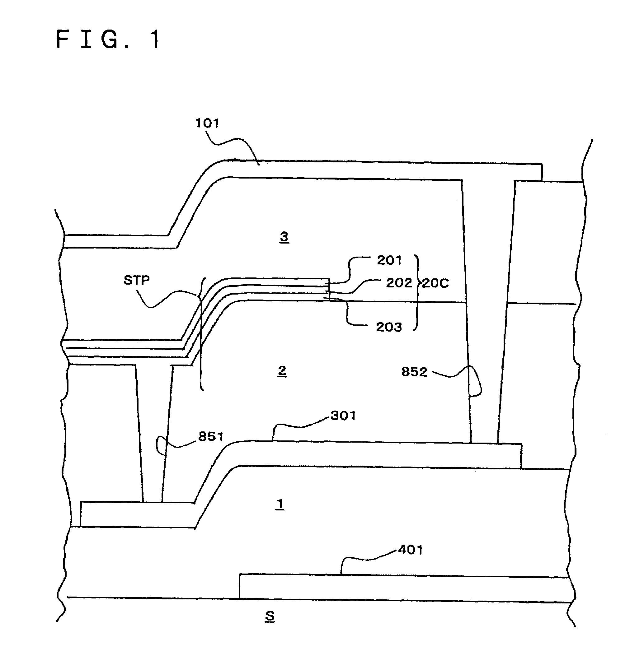
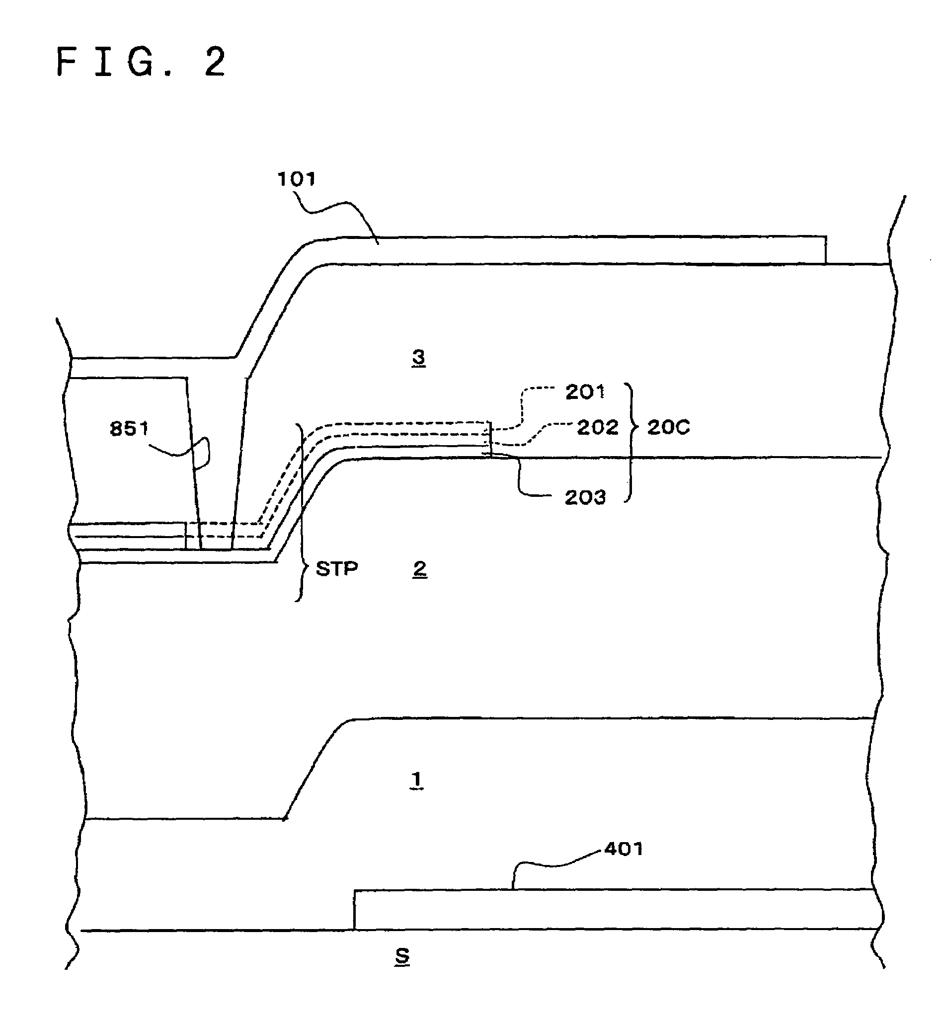
[0077]First, the wiring structure according to this embodiment will be described with reference to FIG. 1. Here, FIG. 1 is a cross-sectional view illustrating one example of the wiring structure related to this embodiment. In FIG. 1, the wiring structure can include wiring 401, a relay layer 301, a capacitor 20C as one example of a laminate as referred to as the present invention, and a conductive layer 101, in order from the bottom side. Further, a third interlayer insulating film 3 is formed between the conductive layer 101 and the capacitor 20C, a second interlayer insulating film 2 is formed between the capacitor 20C and the relay layer 301 an...


PUM


Abstract

The invention provides a wiring structure and a method for manufacturing the same for appropriately establishing an electrical connection between a first conductive layer constituting a part of a laminate and a conductive layer to be electrically connected thereto. The wiring structure can include, on a substrate, a capacitor provided with a first conductive layer, an insulating layer formed on the first conductive layer, and a second conductive layer formed on the insulating layer, a conductive layer electrically connected to the first conductive layer, and a relay layer located below the first conductive layer and the conductive layer, respectively to form a part of laminated structure. The first conductive layer and the conductive layer are electrically connected to each other through the relay layer.

Description

BACKGROUND OF THE INVENTION[0001]1. Field of Invention[0002]The present invention relates to a wiring structure constructed by laminating wiring and circuit elements on a substrate and a method for manufacturing the same. Further, the present invention relates to an electro-optical device provided with such wiring structure.[0003]2. Description of Related Art[0004]A wiring structure of this type can include various circuit elements, such as thin film transistors (TFTs) as switching elements, thin film diodes, capacitors, resistors and the like, and wiring to connect them to each other. Recently, these various elements are frequently constructed three-dimensionally or constructed to form a laminated structure, on a substrate. For example, an arrangement is constructed in such a way that capacitors are arranged on TFTs and wiring electrically connected to the TFTs is formed on the capacitors. This construction permits a high-density wiring structure. As a result, it is possible to ach...

Claims


Application Information

Patent Timeline
IPC IPC(8): G02F1/1343G02F1/133G02F1/1368G02F1/1362G09F9/30H01L21/768
CPCG02F1/136227G02F1/136213G02F1/136209G02F2201/40G02F1/133
Inventor MIYAZAKI, TOSHIHIDEOYAMADA, SHIN
Owner 138 EAST LCD ADVANCEMENTS LTD
Why Eureka
Try Eureka