

Display Device
- Summary
- Abstract
- Description
- Claims
- Application Information
AI Technical Summary
Benefits of technology
Problems solved by technology
Method used
Image

Examples
embodiment 1
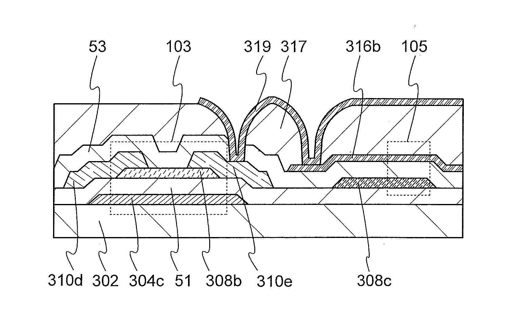
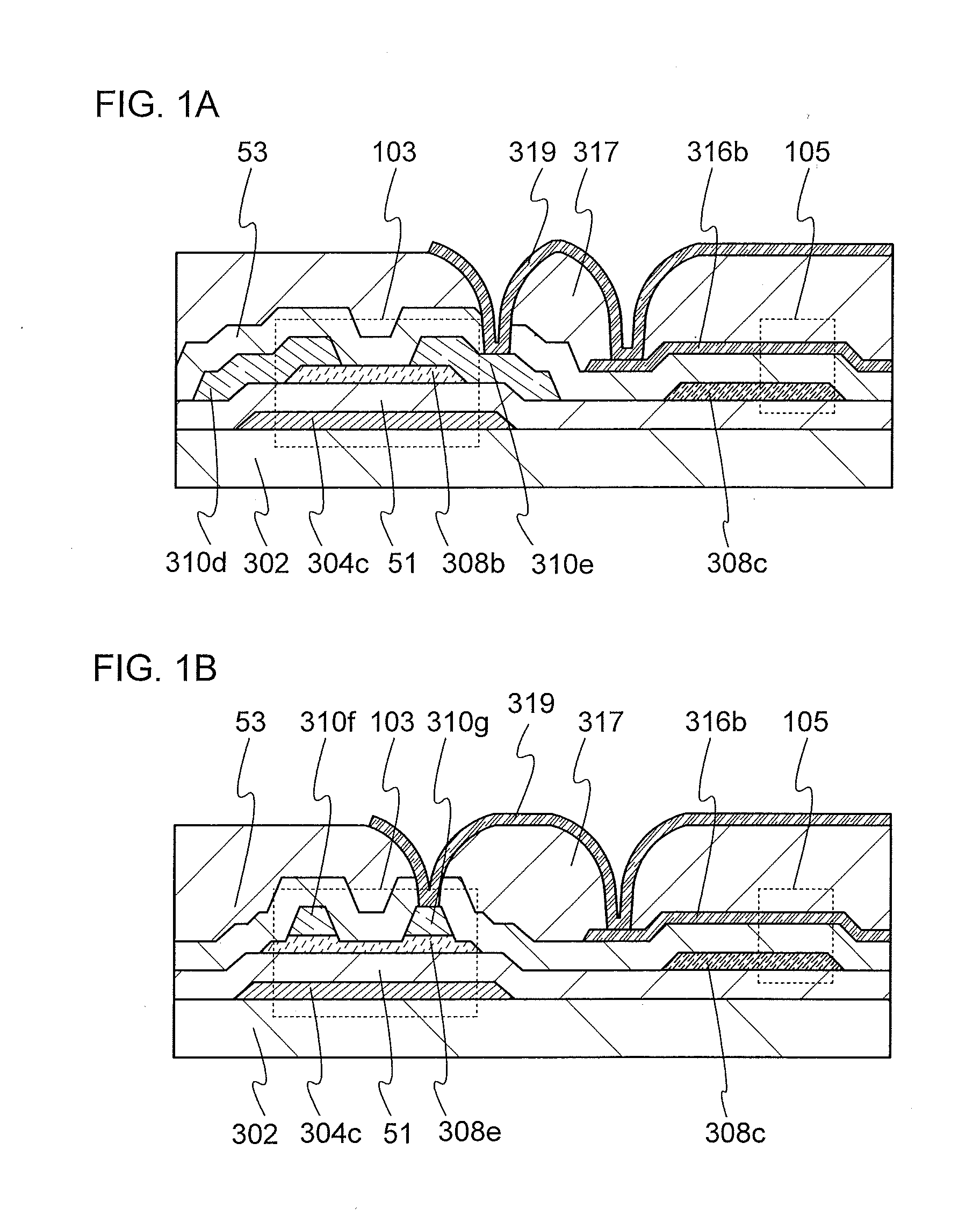
[0091]In the present embodiment, a semiconductor device of one embodiment of the present invention is described with reference to drawings.
[0092]FIGS. 1A and 1B are cross-sectional views illustrating a transistor 103 and a capacitor 105 included in a semiconductor device.
[0093]The transistor 103 illustrated in FIG. 1A includes a conductive film 304c which functions as a gate electrode and is provided over a substrate 302; a gate insulating film 51 framed over the substrate 302 and the conductive film 304c; an oxide semiconductor film 308b which overlaps with the conductive film 304c with the gate insulating film 51 positioned therebetween; and a pair of conductive films 310d and 310e which are in contact with the oxide semiconductor film 308b and function as a source electrode and a drain electrode.
[0094]A metal oxide film 308c is provided over the gate insulating film 51. An inorganic insulating film 53 is provided over the transistor 102 and the metal oxide film 308c. A conductive...
embodiment 2
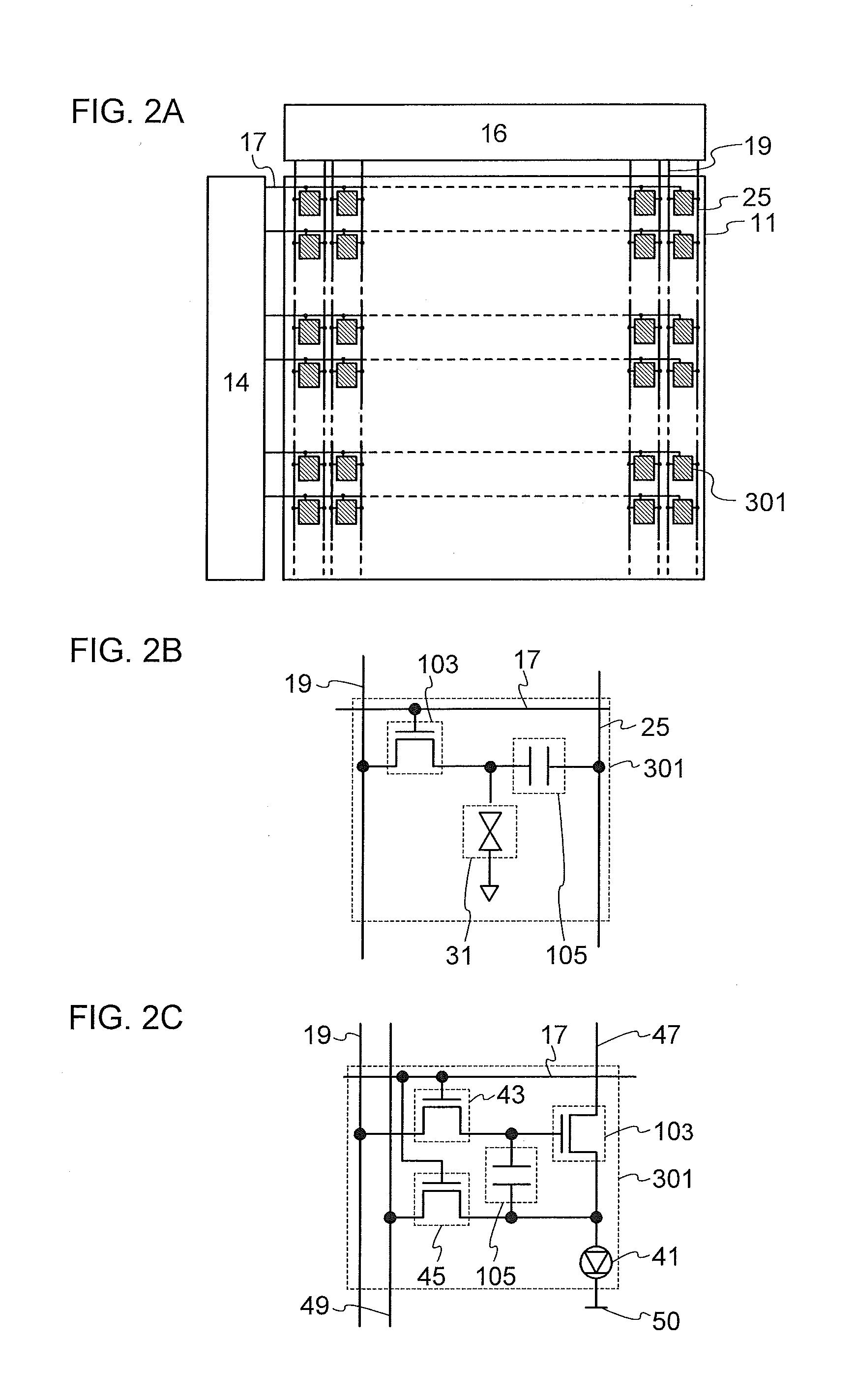
[0113]In this embodiment, a semiconductor device of one embodiment of the present invention and a manufacturing method thereof are described with reference to drawings.
[0114]FIG. 2A illustrates a display device as an example of a semiconductor device. A display device illustrated in FIG. 2A includes a pixel portion 11; a scan line driver circuit 14; a signal line driver circuit 16; in scan lines 17 which are arranged parallel or substantially parallel to each other and whose potentials are controlled by the scan line driver circuit 14; and n signal lines 19 which are arranged parallel or substantially parallel to each other and whose potentials are controlled by the signal line driver circuit 16. The pixel portion 11 further includes a plurality of pixels 301 arranged in a matrix. Furthermore, capacitor lines 25 arranged parallel or substantially parallel are provided along the signal lines 19. Note that the capacitor lines 25 may be arranged parallel or substantially parallel along...
embodiment 3
[0307]In this embodiment, a liquid crystal display device including a transistor different from that described in Embodiment 1 is described with reference to FIG. 11, FIG. 12, FIG. 13, FIG. 14, and FIG. 15.
[0308]A liquid crystal display device illustrated in FIG. 11 includes a transistor 102a with a dual-gate structure in a driver circuit portion illustrated in the cross section A-B.
[0309]The transistor 102a in the driver circuit portion includes the conductive film 304a being over the substrate 302 and functioning as a gate electrode; the insulating films 305 and 306 functioning as the gate insulating film 51; the oxide semiconductor film 308a over the insulating film 306; and the conductive films 310a and 310b functioning as a source electrode and a drain electrode and being in contact with the oxide semiconductor film 308a. The inorganic insulating film 53 is formed over the oxide semiconductor film 308a and the conductive films 310a and 310b, and a conductive film 316d functioni...
PUM
 Abstract
Description
Claims
Application Information