Dynamic phase logic gate

a logic gate and dynamic phase technology, applied in the direction of logic circuits, instruments, pulse techniques, etc., can solve the problems of high interference risk of electronic signals, limited operation speed of electronic devices, and high electronic cross-talk risk

Inactive Publication Date: 2006-08-01
ROMANIUK CHARLES
View PDF38 Cites 20 Cited by
  • Summary
  • Abstract
  • Description
  • Claims
  • Application Information

AI Technical Summary

Benefits of technology

[0014]Another aspect to the present invention provides a logic device for use with data signals comprising optical beams of substantially fixed frequency. The device produces a logical output from at least one of the data inputs. A pair of inputs and a control input each receive a data signal having one of a predetermined set of values....

Problems solved by technology

Electronic devices are limited in operational speeds because of their inherent electrical resistance and capacitance.
A further disadvantage of semiconductor devices is electronic cross-talk, since electronic signals are highly susceptible to interference.
One disadvantage of the current electromagnetic phase devices is that the output ...

Method used


Image

  • Dynamic phase logic gate
  • Dynamic phase logic gate
  • Dynamic phase logic gate

Examples


Embodiment Construction

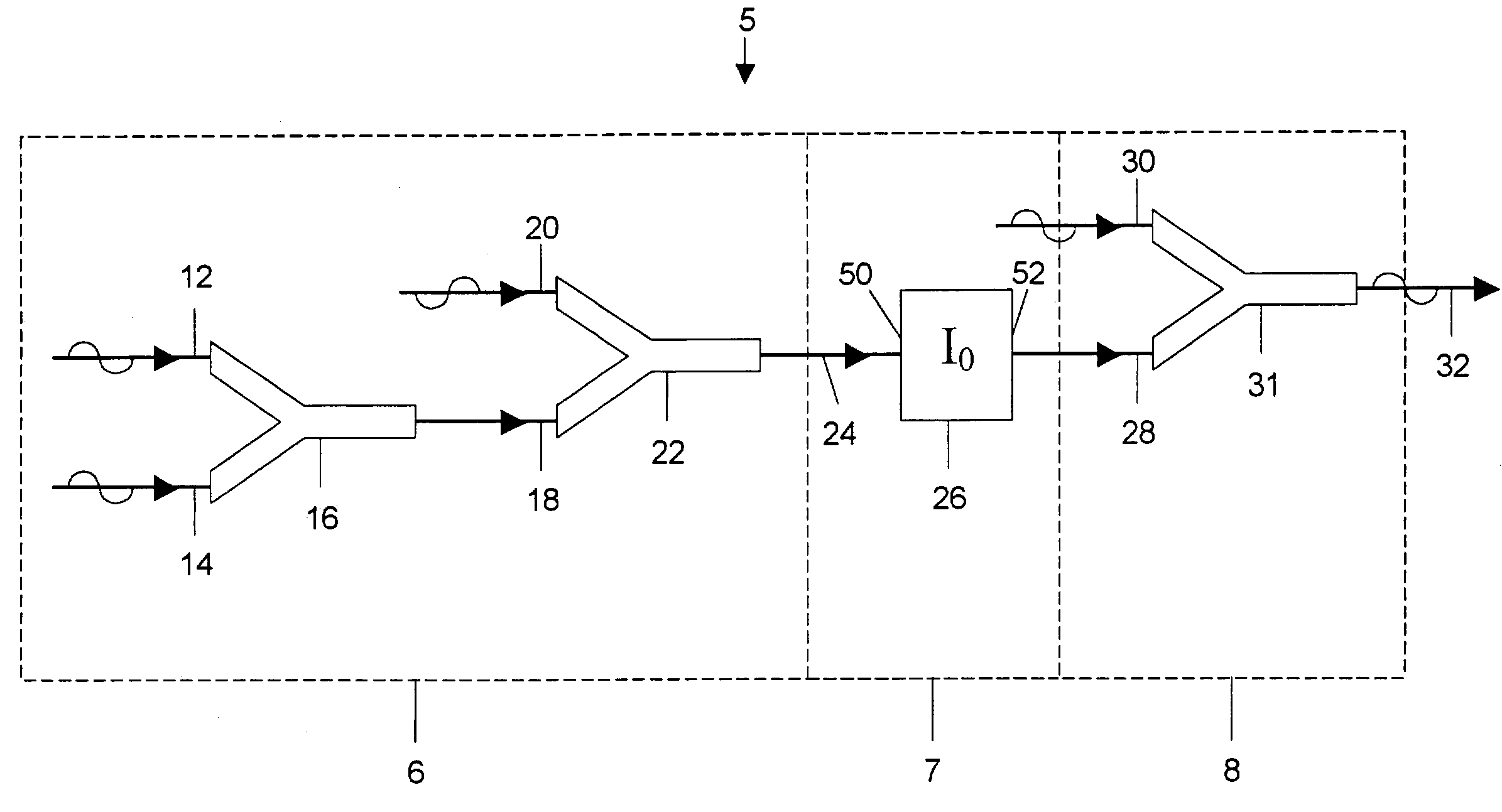
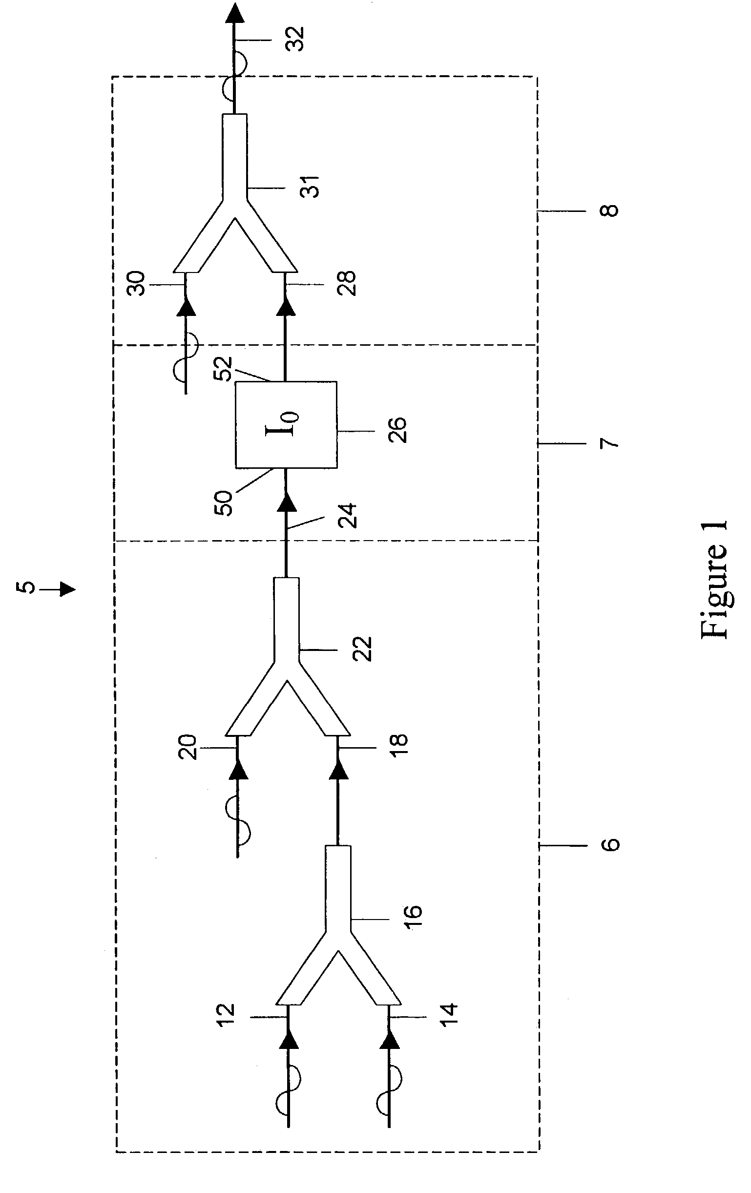
[0036]Referring to FIG. 1, dynamic phase logic gate DPLG 5 includes a first stage 6 for combining a plurality of waveform inputs 12, 14, 20 to produce an intermediate waveform signal 24. Connected to the first stage 6 is a second or filter stage 7, which modifies a wave property of the signal 24 to produce a filtered signal 28. The filter stage 7 is employed to map the analog states of the signal 24 to two binary states represented by the filter signal 28. The filtered signal 28 can then be directed into a third stage 8, which is used to modify the waveform properties of the signal 28 to produce a resultant binary output 32. The output 32 preferably has the same frequency and magnitude as the inputs 12, 14, 20. This facilitates a cascading of several DPLGs 5 in circuits.

AND Gate Example

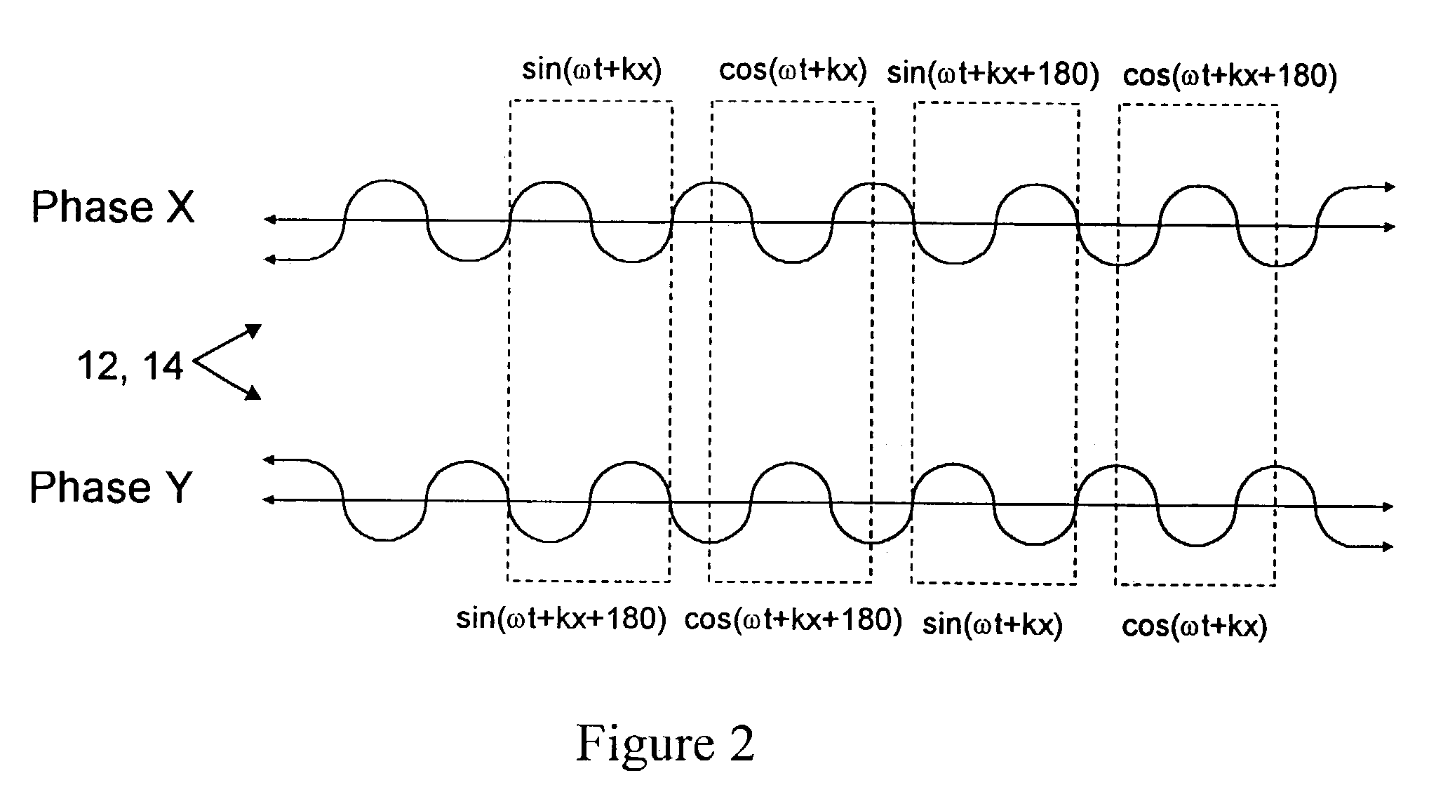
[0037]A variety of functions can be performed by the DPLG 5 based on the waveform properties of the first control input 20, applied in the first stage 6, and a second control input 30, applied in the ...


PUM


Abstract

A logic device for use with data signals having a continuously or semi-continuously varying waveform of substantially fixed frequency. The device provides a logical output from at least one of the data inputs and comprising a first pair of inputs each to receive a data signal having one of a predetermined set of values representing analog, discrete, or digital states. A combiner stage is used to combine the inputs and produce a signal therefrom. A filter stage is utilized to receive the signal and produce a conditioned signal representative of one of a pair of binary states. The conditioned signal is combined with a second control input. The resultant signal is passed to an output.

Description

[0001](This is a continuation of U.S. patent application Ser. No. 09 / 522,912, filed on Mar. 10, 2000 now abandoned)[0002]The present invention relates to logic devices.BACKGROUND OF THE INVENTION[0003]The use of semiconductors to perform logical functions, such as AND, OR or arithmetic functions, is well known in the art. Such semiconductors come in a wide range of sizes, including small scale integrated circuits having 2 to 4 logic gates per package and very large scale integrated circuits, such as microprocessors.[0004]Semiconductor devices do have their shortcomings. Electronic devices are limited in operational speeds because of their inherent electrical resistance and capacitance. A further disadvantage of semiconductor devices is electronic cross-talk, since electronic signals are highly susceptible to interference. Since electrons have electromagnetic fields that can easily interact, two adjacent electronic signals will affect one another, even if they are a significant dista...

Claims


Application Information

Patent Timeline
IPC IPC(8): G06E1/00G02F3/00H03K19/02
CPCH03K19/02G02F3/00
Inventor ROMANIUK, CHARLES
Owner ROMANIUK CHARLES
Why Eureka
Try Eureka