Clock generating circuit

a clock generation and clock technology, applied in the direction of generating/distributing signals, pulse automatic control, instruments, etc., can solve the problems of large fluctuation of the generated clock b>6/b>, enhancing filter precision performance, and difficult integration of low-pass filters

Inactive Publication Date: 2006-08-08
MITSUBISHI ELECTRIC CORP
View PDF13 Cites 30 Cited by
  • Summary
  • Abstract
  • Description
  • Claims
  • Application Information

AI Technical Summary

Problems solved by technology

However, the problem is that the transient phase fluctuation of the generated clock 6 gets large because it is affected by the change in phase of the reference signal 1 upon change of the reference signal 1.
Further, it is hard to integrate the low-pass filter 22 for enhancing filter precision performance because the low-pass filter 22 is generally configured with such as a resistance and a capacitor.
It is difficult to integrate VCXO.
Therefore, the problem is that the phase fluctuation of the generated clock becomes large upon change of the reference signal.
And there is a problem that it is difficult to integrate the low-pass filter or the voltage control oscillator in the case of high precision control of the steady-state phase difference or the transient response upon change of the reference signal.
Still another problem is that the transient response upon change of the reference signal depends upon loop gain in the PLL circuit and the time constant of the low-pass filter, so that high design flexibility cannot be achieved.

Method used


Image

  • Clock generating circuit
  • Clock generating circuit
  • Clock generating circuit

Examples


embodiment 1

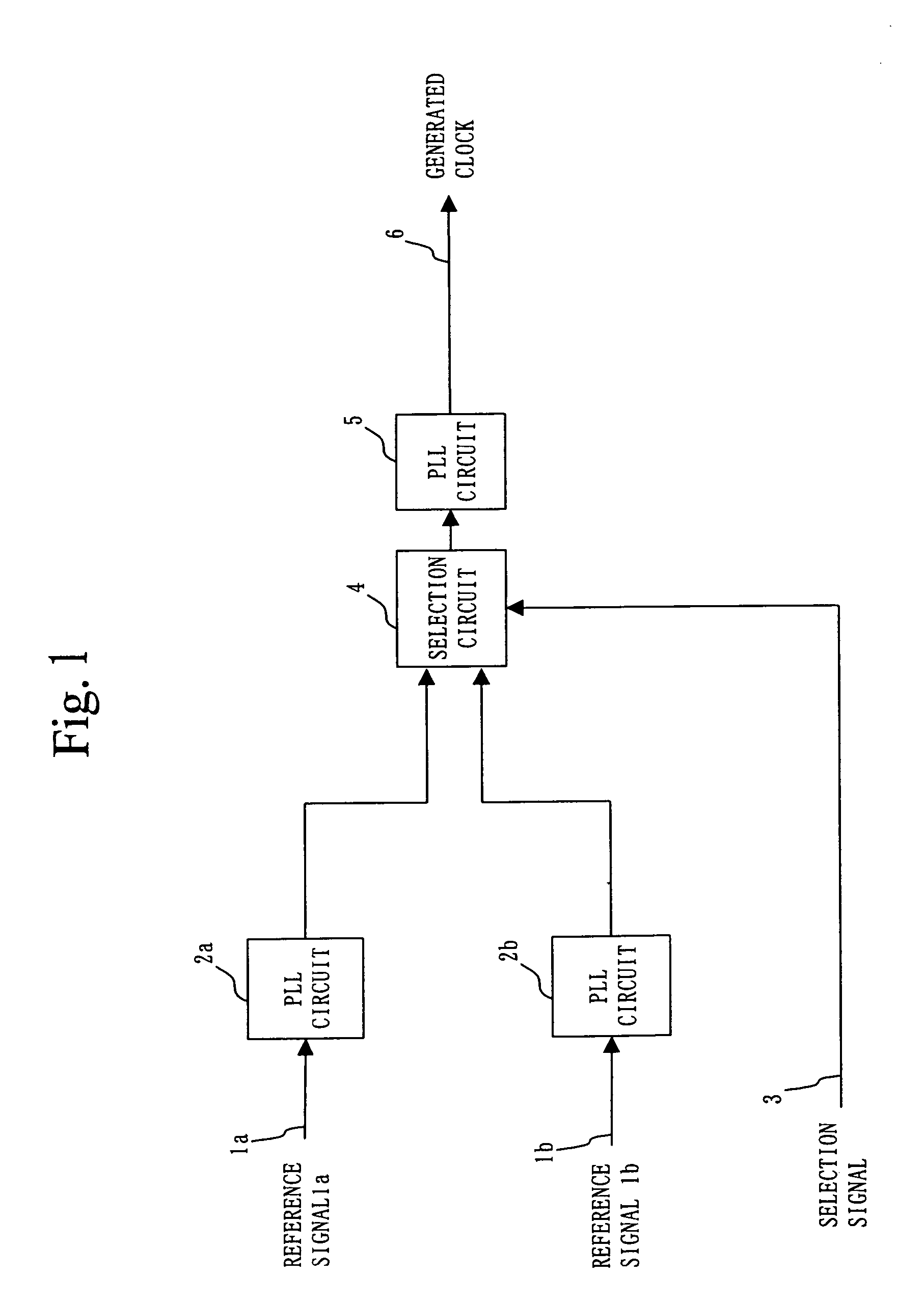
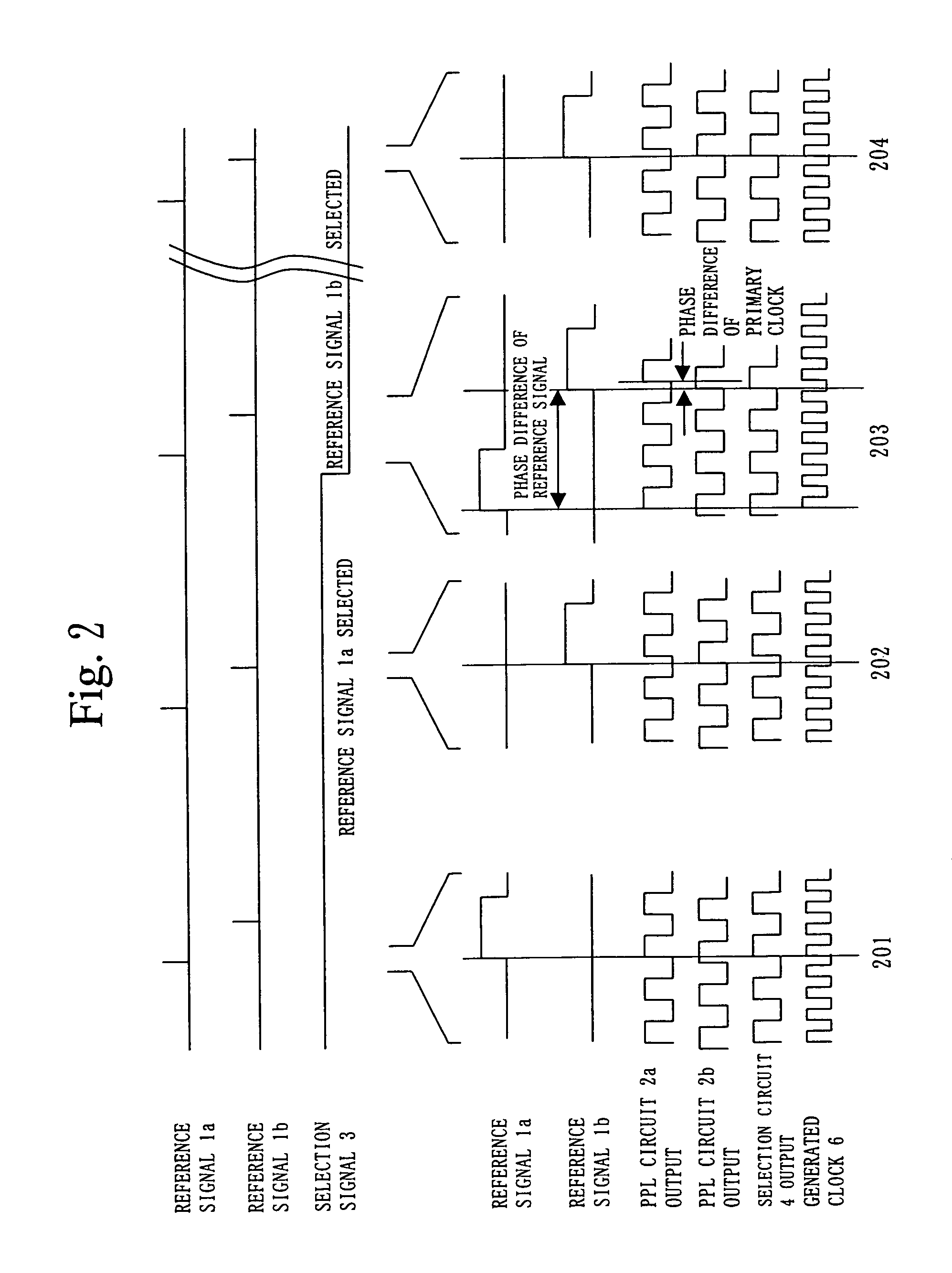
[0033]Hereinafter, a first embodiment is discussed with reference to FIG. 1. With referring to FIG. 1, a reference numeral 1 denotes a reference signal, a reference numeral 2 denotes a PLL circuit, a reference numeral 3 denotes a selection signal, a reference numeral 4 denotes a selection circuit, a reference numeral 5 denotes a PLL circuit, and a reference numeral 6 denotes a generated clock. FIG. 2 shows the waveform of each element in FIG. 1.

[0034]As shown in FIG. 1, the reference signals 1 are inputted, respectively, to the PLL circuits 2. More specifically, a reference signal 1a is inputted to a PLL circuit 2a, and a reference signal 1b is inputted to a PLL circuit 2b. The PLL circuits 2a and 2b output primary clocks that are synchronized, respectively, with the reference signals 1a and 1b inputted.

[0035]Then, the selection circuit 4 selects one of the primary clocks that are synchronized with the reference signals outputted from the PLL circuits 2, respectively, based on the s...

embodiment 2

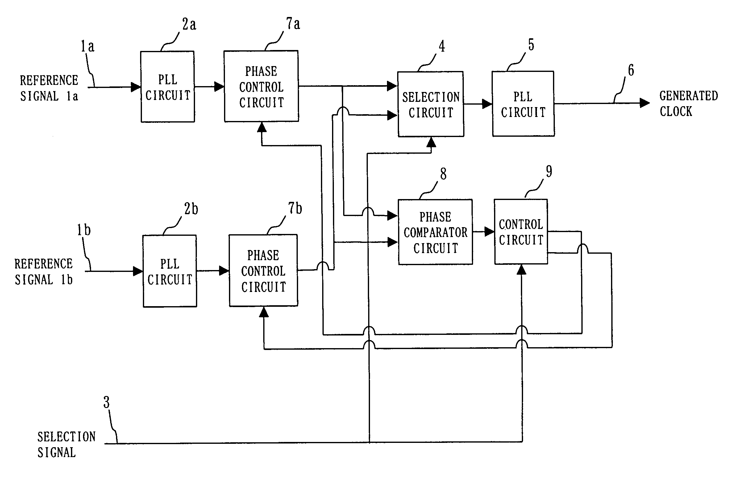
[0043]A second embodiment is now discussed with reference to the drawings. With referring to FIG. 3, a reference numeral 1 denotes a reference signal, a reference numeral 2 denotes a PLL circuit (former stage), a reference numeral 3 denotes a selection signal, a reference numeral 4 denotes a selection circuit, a reference numeral 5 denotes a PLL circuit (latter stage), a reference numeral 6 denotes a generated clock, a reference numeral 7 denotes a phase control circuit, a reference numeral 8 denotes a phase comparator circuit, and a reference numeral 9 denotes a control circuit.

[0044]According to the second embodiment, the phase control circuits 7 are provided, respectively, at the outputs of the PLL circuits 2 receiving the reference signals 1, so that the phase of the primary clock outputted from the phase control circuit 7 through the PLL circuit 2 corresponding to the reference signal 1 selected in the selection circuit 4 based on the selection signal 3 and the phase of the pri...

embodiment 3

[0046]According to a third embodiment, the phase control circuit 7 discussed in the second embodiment is implemented by a ring counter and a selection circuit.

[0047]With referring to FIG. 4, a reference numeral 1 denotes a reference signal, a reference numeral 2 denotes a PLL circuit (former stage), a reference numeral 7 denotes a phase control circuit, a reference numeral 10 denotes flip-flops, a reference numeral 11 denotes a NOR circuit, a reference numeral 12 denotes a selection circuit, a reference numeral 13 denotes a control signal, and a reference numeral 14 denotes an output of the phase control circuit. FIG. 5 shows the waveform of each element in FIG. 4.

[0048]The primary clock outputted from the PLL circuit 2 operates a ring counter that is configured with flip-flops 10 and the NOR circuit 11. As shown in FIG. 5, outputs from a flip-flop 10a˜a flip-flop 10y are multi-phase signals depending upon the number of the stages in the ring counter. Selecting one of the multi-phas...


PUM


Abstract

In a clock generation circuit generating a clock that is synchronized with a reference signal, it is an object to provide stable clocks by controlling phase jitter in a generated clock upon change of the reference signal, eliminate a stable-state phase difference between the reference signal and the generated clock so that control is eliminated, and allow the clock generation circuit to be integrated. The clock generation circuit is configured with multiple stages of PLL circuits such that PLL circuits 2 are provided for reference signals 1, respectively, and one of outputs from the PLL circuits 2 is selected to be fed to a PLL circuit5 provided in a next stage. The phase fluctuation of a signal inputted to the PLL circuit 5 upon change of the reference signal 1 is reduced to control the phase jitter of the generated clock 6, thus allowing high loop gain in both the PLL circuit 2 and the PLL circuit 5. Then, phase difference between the reference signal 1 and the generated clock 6 is eliminated to eliminate control involved, so that the clock generation circuit may be integrated.

Description

TECHNICAL FIELD[0001]This invention relates to a clock generation circuit, which generates a clock that is synchronized with a reference signal in a digital transmission system.BACKGROUND ART[0002]FIG. 9 is the block diagram of a conventional clock generation circuit as an example. With referring to the figure, a reference numeral 1 denotes a reference signal, a reference numeral 3 denotes a selection signal selecting one of a plurality of reference signals, a reference numeral 4 denotes a selection circuit, a reference numeral 5 denotes a PLL circuit, and a reference numeral 6 denotes a generated clock. The PLL circuit is configured with the following elements. A reference numeral 21 denotes a phase comparator, a reference numeral 22 denotes a low-pass filter, a reference numeral 23 denotes an amplifier, a reference numeral 24 denotes a reference voltage generator, a reference numeral 25 denotes a voltage control oscillator, and a reference numeral 26 denotes a divider.[0003]The op...

Claims


Application Information

Patent Timeline
Patent Type & Authority Patents(United States)
IPC IPC(8): H03L7/00H03L7/07H03L7/081H03L7/087
CPCH03L7/07H03L7/087H03L7/0814H03L7/081
Inventor TAKAHASHI, AKIRA
Owner MITSUBISHI ELECTRIC CORP
Why Eureka
Try Eureka