Heat assisted magnetic write element

a write element and heat-assist technology, applied in the field of magnetic elements, can solve the problems of high power consumption of the memory making use of such an external magnetic field, risk of accidental switching, and stability of the magnetization of the free layer

Active Publication Date: 2011-02-24
COMMISSARIAT A LENERGIE ATOMIQUE ET AUX ENERGIES ALTERNATIVES +1
View PDF14 Cites 67 Cited by
  • Summary
  • Abstract
  • Description
  • Claims
  • Application Information

AI Technical Summary

Benefits of technology

[0040]The approach proposed thereby allows maximizing the magnetic torque applied by the magnetic field to the magnetization of the storage layer during its application, because when the magnetization of the storage layer is in the plane, the field is applied at 90° from the magnetization direction (therefore maximum torque allowing a reduction of the amplitude of the field to be applied). Furthermore, this configuration allows minimizing the switching field distributions associated with the fluctuations in shape of the various memory elements which may be encountered with planar-magnetization materials.
[0045]To circumvent this problem, it is advantageous to combine the writing by spin transfer with heat assisted writing. Thanks to the same current passing through the structure, it is possible both to heat the nanostructure and to apply the torque to the magnetization which causes the switching thereof. The temperature rise serves, just at the time of writing, to lower the barrier necessary for the magnetization switching, while preserving a high nonwrite barrier height and therefore good temperature stability.
[0046]Thus a second object of the present invention is to propose an optimal way to implement this combination of heat assisted writing with spin transfer switching. It is also based on the use of out-of-plane magnetization materials, of which the anisotropy switches from out-of-plane to planar under the effect of the heating at the time of writing. However, the spin polarized current generating the spin transfer torque applied to the magnetization of the nanostructure is and remains out-of-plane of the nanostructure at all the operating temperatures of the device. Thus the spin polarization is perpendicular to the magnetization direction of the storage layer at the most crucial moment of the write process (that is around the maximum temperature reached by the magnetic element during writing) which serves to maximize the spin transfer efficiency and thereby minimize the current density required for writing. In fact, the latter varies approximately with the sine of the angle between the direction of current polarization and the magnetization of the nanostructure, in particular in the case of magnetic tunnel junctions.
[0085]Furthermore, the fact of using heat assistance serves to have a better thermal stability of the magnetization on standby (nonwrite) because the out-of-plane magnetic anisotropy can be selected to be very high at the standby temperature according to the principle of Heat Assisted Magnetic Recording (HAMR) well known to a person skilled in the art.

Problems solved by technology

Since the switching field distribution function for all the memory points is wide (in fact, this distribution is wide due to the manufacturing imperfections, particularly associated with the etching of the memory points and the intrinsic statistical fluctuations associated with the thermally activated magnetization fluctuations), it is necessary for the magnetic field on the selected memory point to be higher than the highest switching field of the distribution, at the risk of accidentally switching certain memory points located on the line or on the corresponding column, where the switching field located in the lower part of the distribution is lower than the magnetic field generated by the line or column alone.
Furthermore, the power consumption of the memory making use of such an external magnetic field is commensurately higher with a wider switching field distribution.
Another drawback of these prior art memories concerns the stability of the magnetization of the free layer with regard to thermal fluctuations as the size of the memory point decreases.
In doing so, however, the magnetic field required for magnetic switching increases, due to a higher power consumption to generate the field necessary for the magnetic switching.
The heat assisted write approaches described nevertheless have defects.
However, any difference from a perfectly circular cross section, for example associated with etching defects, is liable to cause a shape anisotropy of a few mT again yielding the need to increase the write field.
Once again, when the cross section of the conducting lines is reduced to increase the density of the memories or logic circuits, the problem arises of the electromigration limit in the conducting line.
Furthermore, when the magnetic switching takes place by spin transfer, the current densities required are high, typically in the range of a few 106 A / cm2, thereby subjecting the tunnel barrier to a high electrical stress.
Reading is carried out at a lower current density than writing, so that the temperature rise is insufficient to cause the switching of the magnetization of the storage layer.
However, to simply use the spin transfer effect during writing raises the problem of the thermal stability of the magnetic element in very small dimensions.
It is well known to a person skilled in the art that if the temperature fluctuations given by KBT represent a significant fraction of KV, then the magnetization of the nanostructure becomes unstable with regard to the temperature fluctuations, so that the nanostructure can no longer store the data inscribed in the orientation of its magnetization.
Increasing the shape factor of the nanostructure excessively (for example by giving it an elliptical shape with a major axis / minor axis shape ratio above 2) does not help to solve the problem, because the magnetization is then switched by wall propagation nucleation and no longer by coherent switching.
However, the spin polarized current generating the spin transfer torque applied to the magnetization of the nanostructure is and remains out-of-plane of the nanostructure at all the operating temperatures of the device.
Reading is carried out a lower current density than writing, so that the temperature rise and / or spin transfer applied to the nanostructure are insufficient to cause the switching of its magnetization.

Method used


Image

  • Heat assisted magnetic write element
  • Heat assisted magnetic write element
  • Heat assisted magnetic write element

Examples


Embodiment Construction

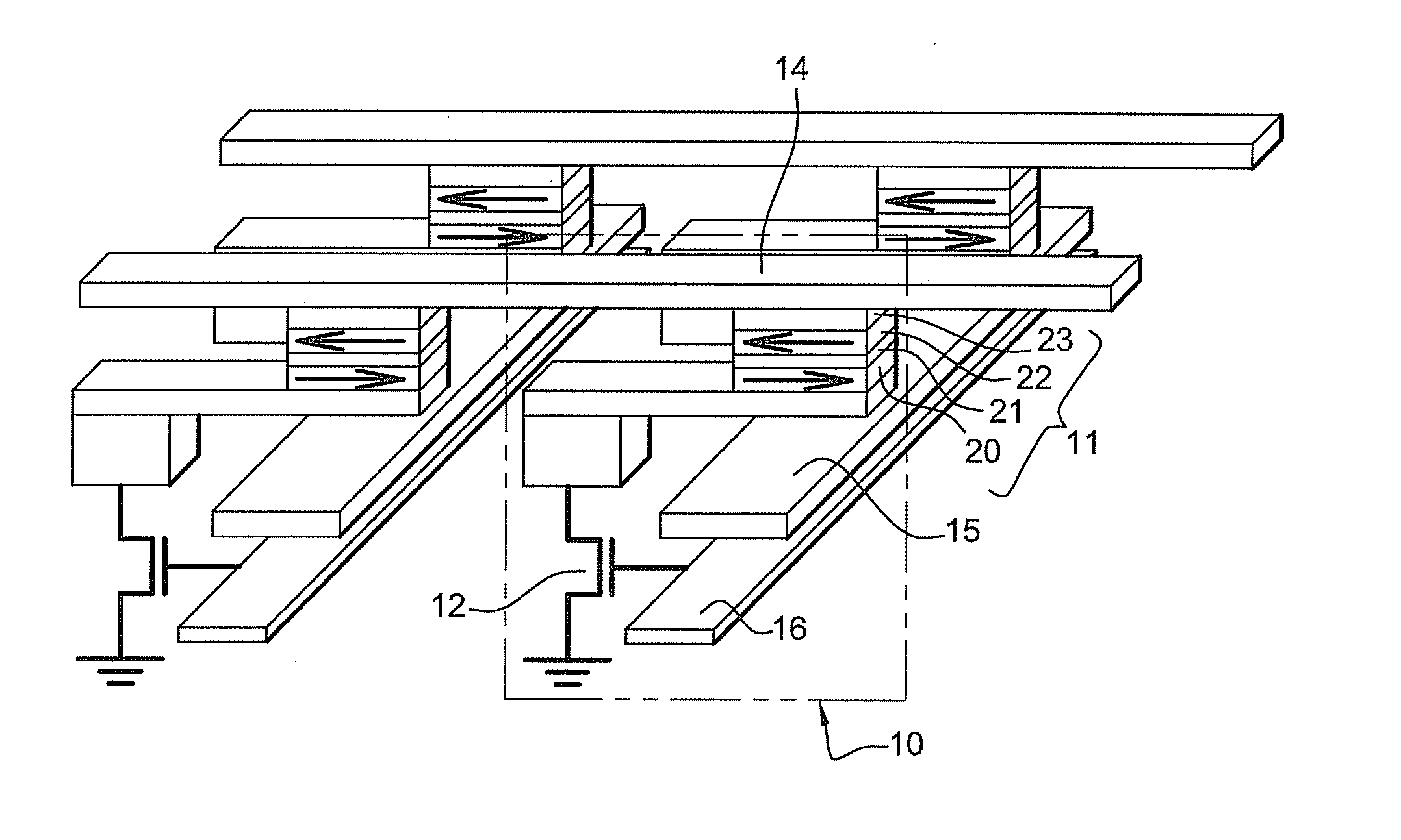
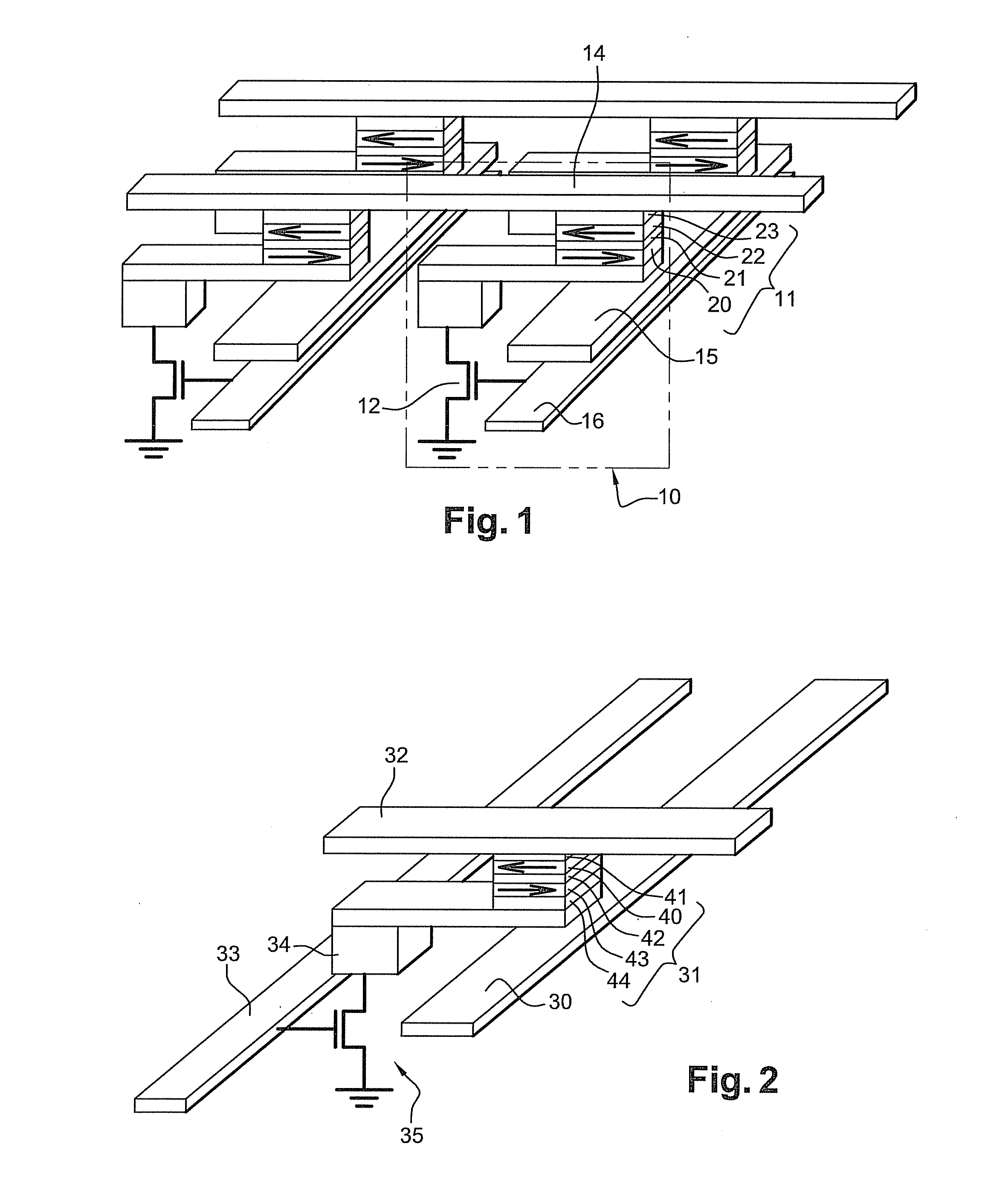
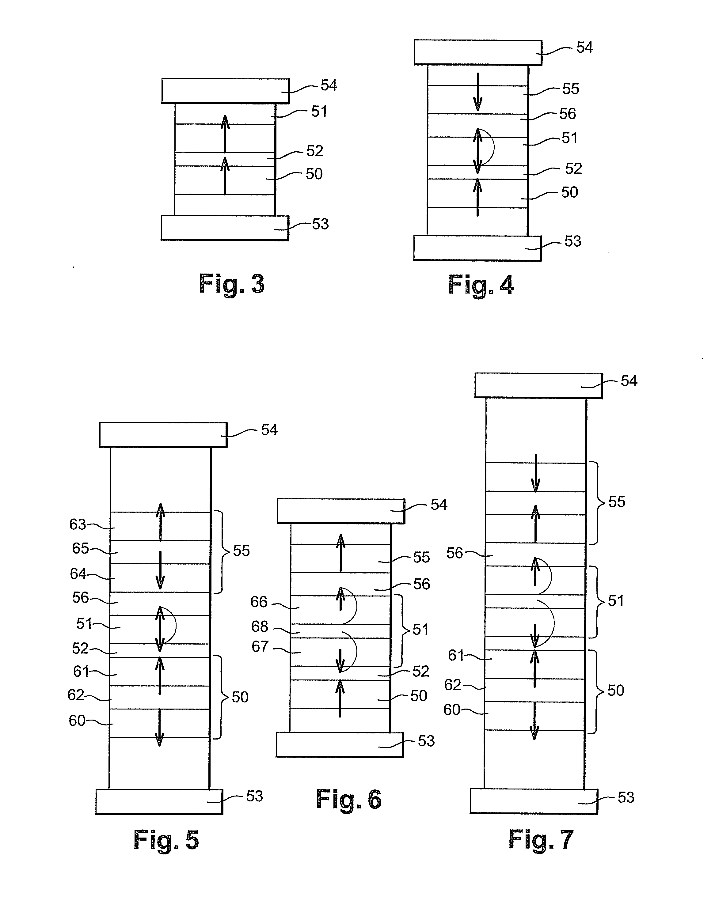
[0099]The magnetic element at the core of the memory point or the logic element of the invention is a magnetoresistive element using the giant magnetoresistance or tunnel magnetoresistance effect. The core of this magnetoresistive element basically comprises a sandwich formed of two magnetic layers 50, 51 separated by a non magnetic spacer 52.

[0100]According to the invention, the two magnetic layers have a nonwrite anisotropy perpendicular to the plane of the layers.

[0101]The fixed magnetization layer or reference layer 50 has magnetic properties such that its magnetization remains perpendicular to the plane throughout the temperature range in which the magnetic element operates (in particular during writing and especially during reading and on standby). This operating temperature range may extend from as low as desired to typically +250° C. at the time of writing. There is no lower temperature limit for the operation of a fixed magnetization layer because the out-of-plane anisotrop...


PUM


Abstract

This magnetic element for writing by magnetic field or heat assisted spin transfer comprises a stack consisting of:a free magnetic layer, also called storage layer or switchable magnetization layer (51), of which the magnetization direction is switchable between two nonwrite stable states, both directed out-of-plane and substantially perpendicular to the plane of said layer, and of which the magnetization is spontaneously reoriented from substantially perpendicular to the plane to substantially in the plane under the effect of the rise in temperature during the writing;at least one reference magnetic layer (50, 55), called pinned layer, of which the magnetization is oriented substantially perpendicular to the plane of said layer;a nonmagnetic spacer (52) inserted between the two layers;means for making an electric current flow perpendicular to the plane of said layers.

Description

TECHNICAL FIELD[0001]The present invention relates to the field of magnetic elements incorporating a magnetoresistive stack comprising two magnetic layers separated by an insulating tunnel barrier, a confined-current-path layer, a semiconducting layer or a metal layer, and in particular, a magnetic tunnel junction, such as those used in nonvolatile magnetic random access memories, which permit, in a manner known per se, the storage, reading and writing of data in electronic systems. More specifically, it applies to magnetic random access memories, designated conventionally by the acronym MRAM, consisting of a set of memory points each formed by a magnetic tunnel junction, also designated by the acronym MTJ. In a similar manner, the present invention also relates to logic elements having magnetic layers, insofar as they use at least one magnetoresistive stack comprising two magnetic layers separated by an insulating tunnel barrier, a confined-current-path layer, a semiconducting laye...

Claims


Application Information

Patent Timeline
Patent Type & Authority Applications(United States)
IPC IPC(8): G11C11/14
CPCB82Y25/00G11C11/16H01F10/3254H01F10/3286H01F10/3272H01L27/222H01L43/08H01F10/3263H10B61/00H10N50/10
Inventor DIENY, BERNARD
Owner COMMISSARIAT A LENERGIE ATOMIQUE ET AUX ENERGIES ALTERNATIVES
Why Eureka
Try Eureka