

Semiconductor memory
a technology of semiconductor devices and memory, applied in the field of semiconductor memory, can solve the problems of information loss, information stored in the capacitor must be renewed, information loss is also caused, etc., and achieve the effect of short switching time and low programming voltag
- Summary
- Abstract
- Description
- Claims
- Application Information
AI Technical Summary
Benefits of technology
Problems solved by technology
Method used
Image

Examples
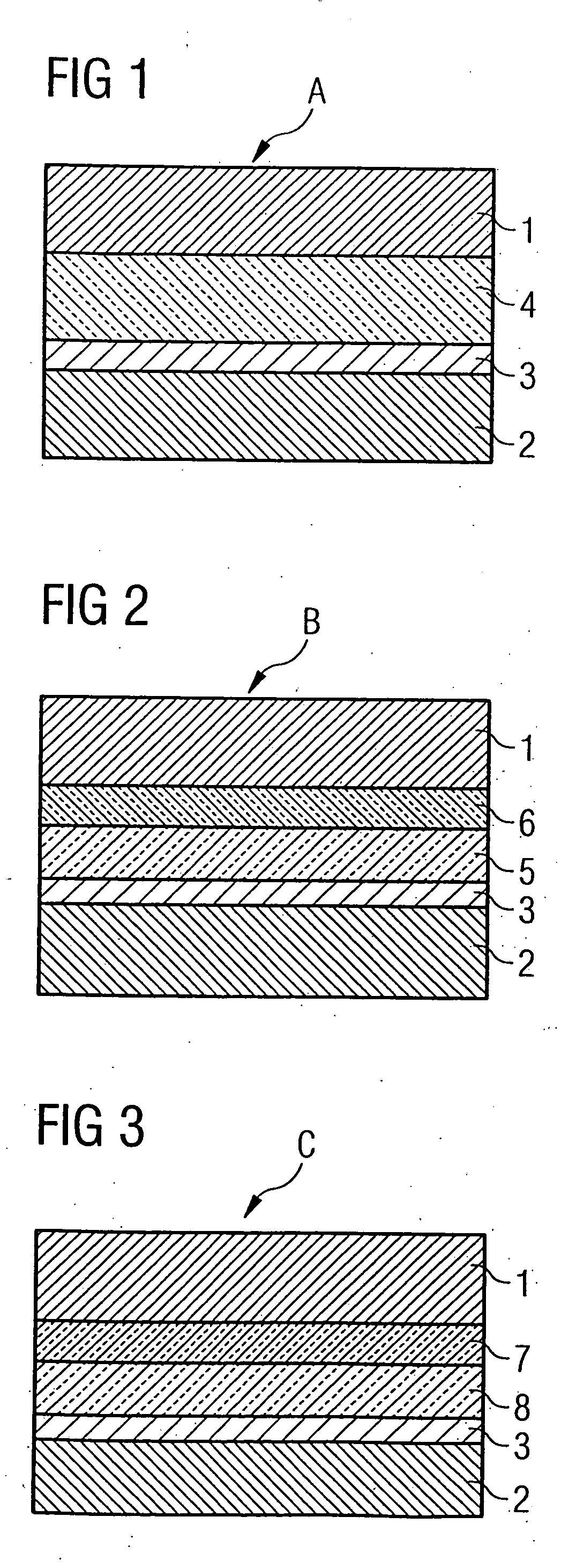
first embodiment
[0033] The amorphous, micromorphous or microcrystalline silicon material 4 used in the first embodiment preferably comprises one of the following compounds: amorphous Si:H, amorphous Si:C, H, amorphous Si:H, O, μc-Si, or SiOx (x=1 . . . 2), wherein other (foreign) components may also be added as alloys, e.g. amorphous Ge:H or materials derived therefrom.
[0034]FIG. 2 shows the schematic layer structure of a second preferred embodiment of the inventive non-volatile memory cell B that has a resistively switching property on the basis of ion drift. According to this second preferred embodiment, the resistively switching, non-volatile memory cell comprises—instead of the amorphous, micromorphous or microcrystalline silicon matrix material layer 4 doped with alkali, earth alkali or metal ions—a double layer 5, 6 with a strongly ion-doped silicon layer 5 and a silicon layer 6 that is non-doped with respect to highly movable alkali, earth alkali and metal ions.
[0035] Consequently, the resi...
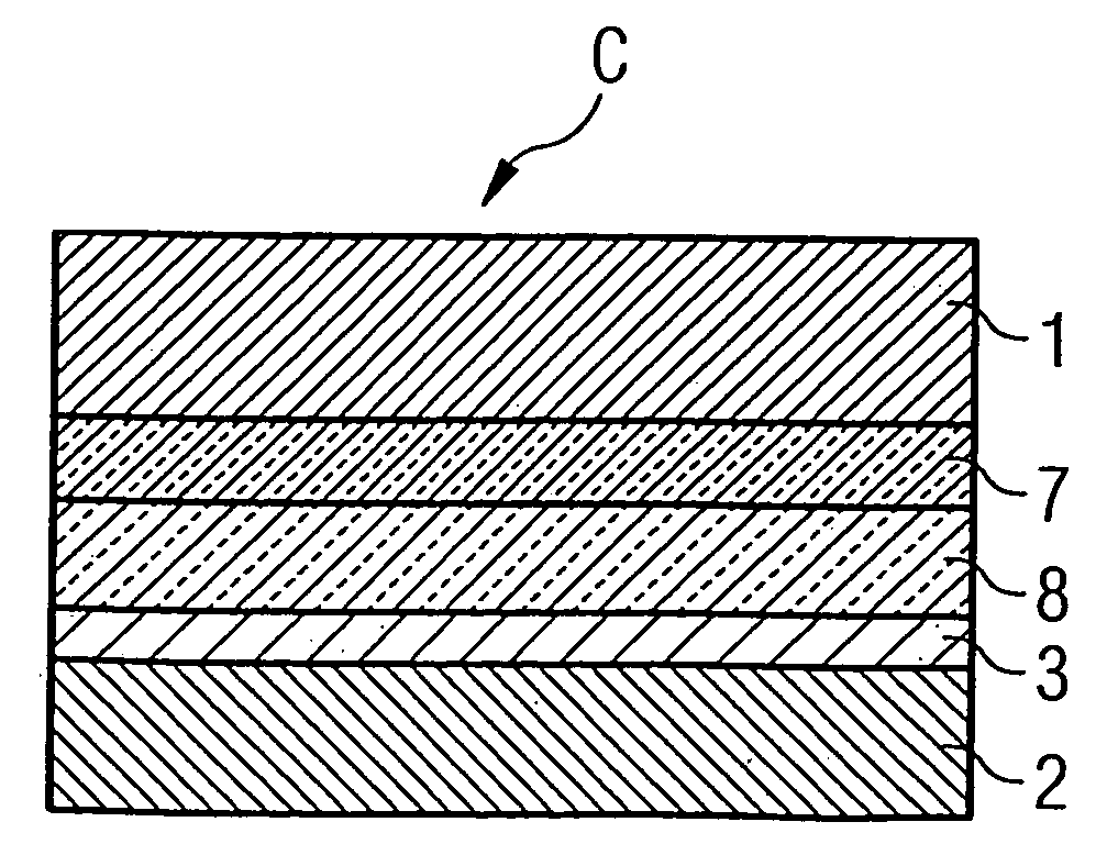
third embodiment
[0048] Alternatively, in this third embodiment, the double layer 7, 8 may also be designed as a single silicon layer comprising a doping profile that proceeds from strong doping to weak doping.
[0049] The inventive memory cell A, B, C is preferably manufactured by a CMOS process-compatible method. The layer arrangements described above may optionally be realized in horizontal or in vertical design on a semiconductor substrate and are independent both of the selected electrode materials and of the choice of an amorphous, micromorphous or microcrystalline silicon diffusion matrix. Electrode materials that generate an ohmic contact to amorphous Si-layers have already been known. The electrode materials are preferably manufactured of inert or refractory elements such as W, Mo, or Ti, which establish a good ohmic contact to the silicon matrix materials doped with highly movable ions.
[0050] According to a further aspect of the present invention, there is a method for manufacturing a resis...
PUM
 Abstract
Description
Claims
Application Information