THz (Terahertz) wave modulator

A modulator and semiconductor technology, applied in detection and imaging, terahertz communication, can solve the problems of long, limited and complicated preparation process

Inactive Publication Date: 2013-04-10
SOUTHEAST UNIV
View PDF1 Cites 28 Cited by
  • Summary
  • Abstract
  • Description
  • Claims
  • Application Information

AI Technical Summary

Problems solved by technology

However, due to the short recombination life of carriers in GaAs, the response time is about 130 ps, ​​so although the modulation rate of terahertz waves can reach GHz in theory, in order to obtain higher photogenerated carriers Concentration and large modulation depth, the luminous flux of the 810nm modulated laser needs to reach 0.8μJ / cm 2 The extremely high level, and its corresponding continuous wave output laser power needs to reach 10 5 W above, which makes this kind of modulator is greatly limited in practical applications
[0004] see figure 1 Recently, researchers have proposed a high-speed terahertz wave modulator based on high electron mobility transistors and metamaterial structures, but the layer structure of this kind of high electron mobility transistors is more complicated than that of metal oxide semiconductor field effect transistors, and the preparation process Long, high cost, and its large parasitic capacitance limits the modulation rate of the modulator

Method used


Image

  • THz (Terahertz) wave modulator
  • THz (Terahertz) wave modulator
  • THz (Terahertz) wave modulator

Examples


Embodiment Construction

[0017] In order to make the technical means, creative features, goals and effects achieved by the present invention easy to understand, the present invention will be further described below in conjunction with specific embodiments.

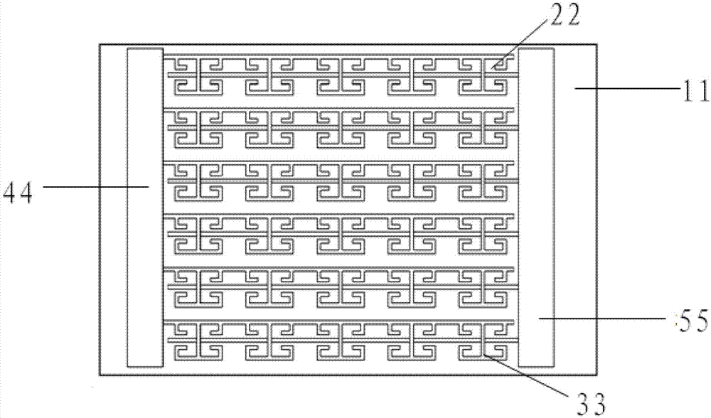
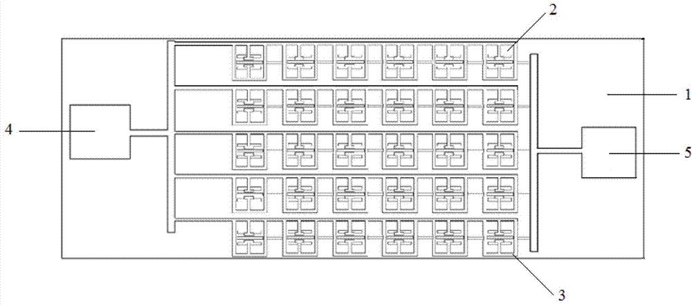
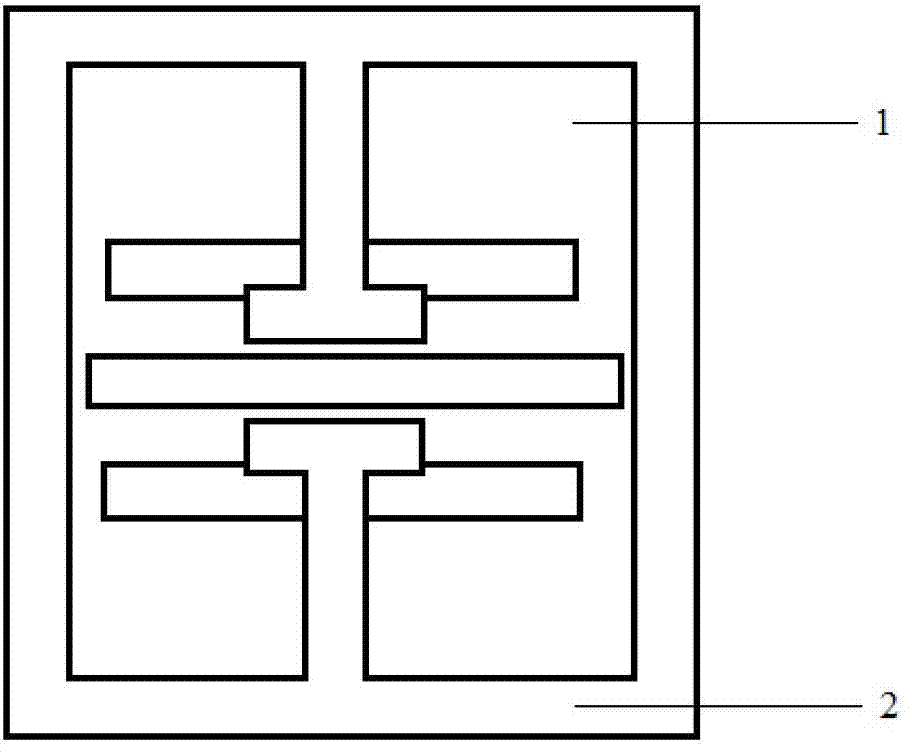
[0018] see figure 2 and image 3 , the terahertz modulator of the present invention includes a semiconductor substrate 1 through which terahertz waves are permeable, a metal oxide semiconductor field effect transistor array 2 distributed periodically on the semiconductor substrate 1, and a metal oxide semiconductor field effect transistor array 2 on the semiconductor substrate 1. The metamaterial resonant unit array 3 , the first metal plate 4 and the second metal plate 5 prepared on the array 2 . The metal oxide semiconductor field effect transistor array 2 and the metamaterial resonant unit array 3 are connected by metal wires.

[0019] Wherein, the first metal plate 4 is connected to the source and drain of the MOSFET; the second metal plate...


PUM

PropertyMeasurementUnit
thicknessaaaaaaaaaa

Abstract

The invention discloses a THz (Terahertz) wave modulator. The THz wave modulator comprises a semiconductor substrate (1), MOSFET (Metal-Oxide-Semiconductor Field Effect Transistor) arrays (2), metamaterial resonance unit arrays (3), a first metal plate (4) and a second metal plate (5), wherein THz wave can permeate the semiconductor substrate (1), the MOSFET arrays (2) are distributed on the semiconductor substrate (1) according to a certain period, the metamaterial resonance unit arrays (3) are prepared on the MOSFET arrays (2), the first metal plate (4) is connected with a source electrode and a drain electrode of each MOSFET, and the second metal plate (5) is connected with a grid electrode of each MOSFET. According to the THz wave modulator disclosed by the invention, the working voltage of the MOSFET is very low, and thus the THz wave modulator prepared by the MOSFET can work under low voltage; and the switching time of the MOSFET is extremely short, the magnitude order of the switching time is 10-100ns, and thus the modulating rate of the THz wave modulator prepared by the MOSFET is larger than 10MHz.

Description

technical field [0001] The invention relates to a modulator, in particular to a terahertz wave modulator, and belongs to the fields of terahertz communication, detection and imaging. Background technique [0002] Terahertz (THz) waves refer to electromagnetic waves from 0.1THz to 10THz, with a wavelength in the range of 0.03mm-3mm, between microwave and infrared. Compared with electromagnetic waves in other bands, terahertz waves have the characteristics of small photon energy and strong penetrating power, which has brought profound impacts on the fields of communication, military, medicine, security inspection and so on. Among them, a high-speed terahertz wave modulator with a modulation rate greater than 10 MHz is one of the essential devices in a terahertz communication system, but the current modulation rate of a terahertz wave modulator is mainly limited by the performance of the substrate material and the device structure. [0003] Among the terahertz wave modulators ...

Claims


Application Information

Patent Timeline
Patent Type & Authority Applications(China)
IPC IPC(8): G02F1/355
CPCG02F1/015G02F2202/30G02F2203/13G02F2203/15
Inventor 张雄廖民亮丛嘉伟崔一平
Owner SOUTHEAST UNIV
Why Eureka
Try Eureka