Electrostatically actuated low response time power commutation micro-switches

a micro-switching and power commutation technology, applied in the field of micro-system components, can solve the problems of reducing the lifetime of the device, limiting the radiofrequency power that can pass through the membrane thus produced, and the stiffness of the membrane then requires a larger force to move. , to achieve the effect of low response tim

Inactive Publication Date: 2007-11-20
THALES SA
View PDF8 Cites 29 Cited by
  • Summary
  • Abstract
  • Description
  • Claims
  • Application Information

AI Technical Summary

Benefits of technology

[0014]The invention proposes a novel architecture and a novel production process for obtaining a microswitch that can withstand a significant RF (radiofrequency) power and possesses a low response time, while still maintaining control voltages of around a few volts to a few tens of volts.

Problems solved by technology

This is because the direct contact between the membrane and the conducting surfaces or the control electrode appreciably reduces the lifetime of the device.
The main drawback of this technique is that the deposited layers necessarily have a small thickness, the stack of layers amounting to a few microns, thereby limiting the radiofrequency power that can pass through the membrane thus produced.
Unfortunately, the increased stiffness of the membrane then requires a larger force to move it, and consequently also a higher actuating voltage.

Method used


Image

  • Electrostatically actuated low response time power commutation micro-switches
  • Electrostatically actuated low response time power commutation micro-switches
  • Electrostatically actuated low response time power commutation micro-switches

Examples


first embodiment

[0076]FIGS. 3, 4, 5 and 6 show the various steps of the process for producing the parallel-type microswitch according to a

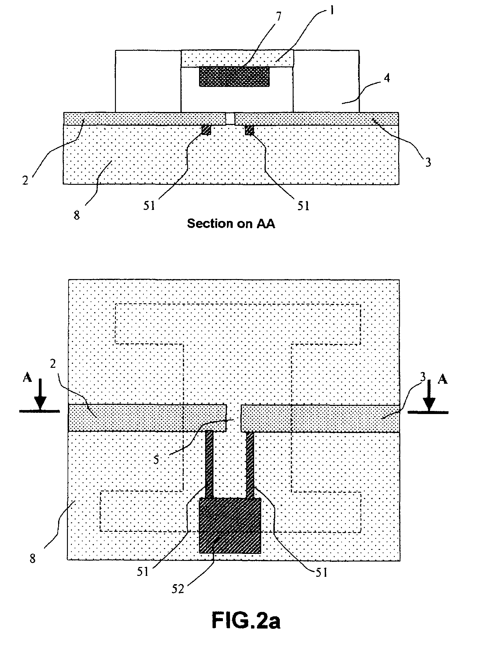
[0077]FIG. 3 shows a top view and two sectional views on AA and BB of the first subassembly 100 before assembly. The process for fabricating the first subassembly typically comprises the following steps:[0078]production on an insulating substrate 8, for example made of insulating silicon or glass, of regions 81 of additional thickness, called mesas, by etching said substrate;[0079]production of a layer 9 of insulating material of the silica type on the surface of the substrate 8, which includes the mesas if the substrate is not sufficiently insulating. This layer may be obtained by deposition or by surface oxidation of the substrate, especially in the case of a silicon substrate;[0080]simultaneous production of the control lines 51, the control pad 52 and the control electrode 5. This control electrode may optionally be covered by the input and output signal line...

second embodiment

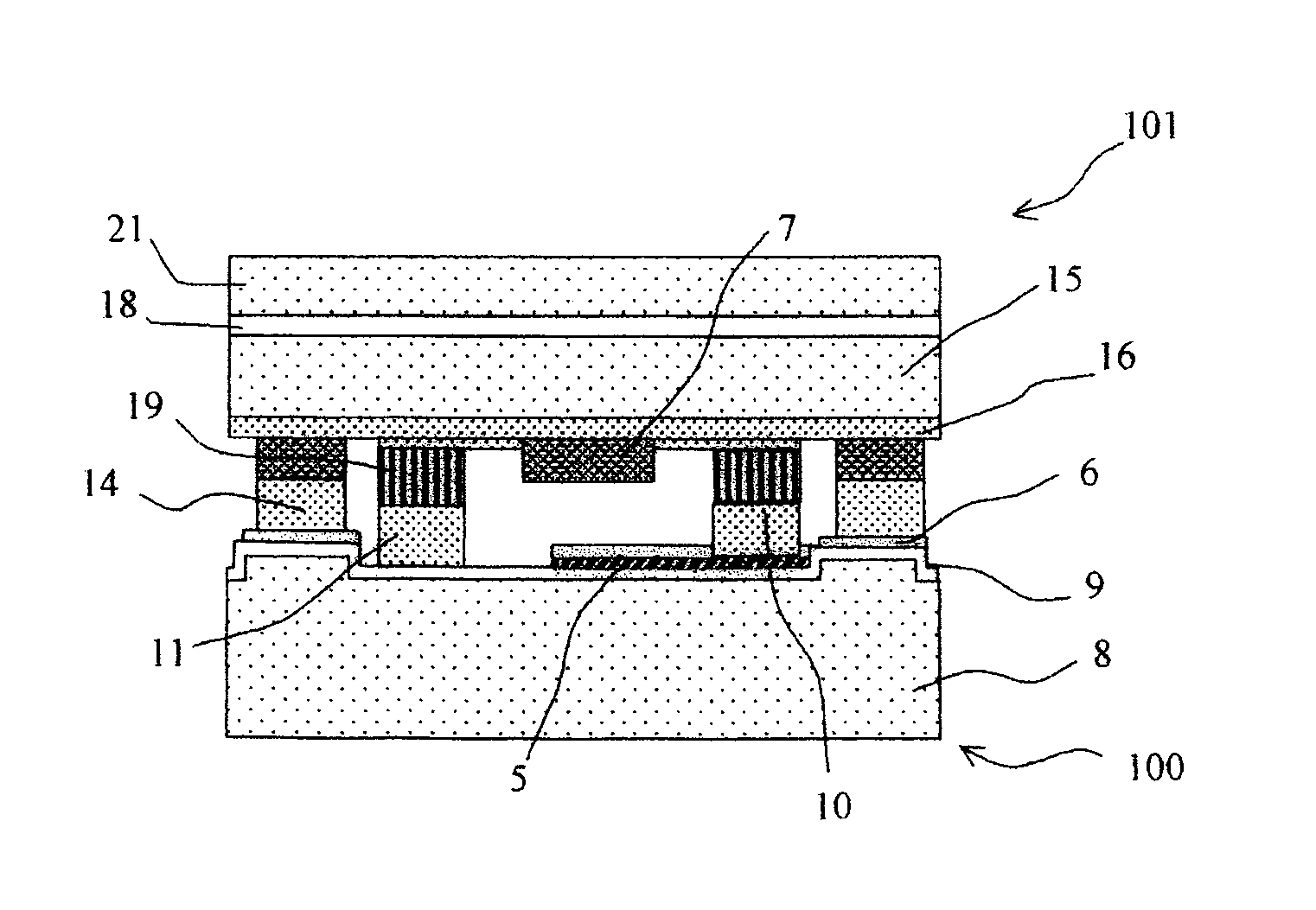
[0095]FIGS. 7, 8 and 9 show the various steps of the process for producing a parallel-type microswitch in a

[0096]FIG. 7 shows a sectional view of the first subassembly 100 before assembly. The process for fabricating said first subassembly typically comprises the following steps:[0097]simultaneous production of the control line 51, the control pad 52 and the control electrode 5. This control electrode may optionally be covered by the input and output signal lines 2 and 3. The control line 51 is sufficiently resistive to prevent the propagation of the RF signal. Typically, this resistance is greater than one hundred ohms / square;[0098]deposition of a layer 6 of insulating material of the silicon nitride or silicon oxide type, covering the lines 51 and, optionally, partly the electrode 5; and[0099]simultaneous production of:[0100]two conducting lines 10 and 11 implanted on said substrate 8, these being called ground lines, which are mutually parallel and electrically connected to an el...


PUM


Abstract

The field of the invention is that of microsystems of the electrostatically actuated microswitch type that are used in electronics to carry out switching functions, especially in the microwave field for mobile telephony and radars. The object of the invention is to improve the performance of the switch by reducing the response time of the device and by increasing the radiofrequency or microwave power supported, while still maintaining low switching voltages. This improved performance is obtained by using thick membranes and by placing a material of high relative permittivity between said membrane and the associated electrode. The switch is obtained by a novel production process, the membrane being produced on an independent substrate and then joined to the base substrate of the switch. Examples of processes for producing devices according to the invention with the materials that can be used, the possible geometries and the various production steps are given.

Description

CROSS-REFERENCE TO RELATED APPLICATIONS[0001]The present Application is based on International Application No. PCT / FR2003 / 002835, filed on Sep. 26, 2003, which in turn corresponds to FR 02 / 12007 filed on Sep. 27, 2002, and priority is hereby claimed under 35 USC § 119 based on these applications. Each of these applications are hereby incorporated by reference in their entirety into the present application.FIELD OF THE INVENTION[0002]The field of the invention is that of microsystem components also called MEMS (the acronym for MicroElectroMechanical Systems) and more particularly to radiofrequency or microwave microswitches incorporating a membrane that can deform under the action of an electrostatic field. The main fields of application are wireless telecommunication systems and radars.DESCRIPTION OF THE PRIOR ART[0003]Microsystem components have been developed in recent years from the technologies used for producing electronic circuits. FIG. 1 shows a diagram illustrating the princ...

Claims


Application Information

Patent Timeline
Patent Type & Authority Patents(United States)
IPC IPC(8): H01L21/00H01H59/00
CPCH01G5/16H01H59/0009
Inventor ZIAEI, AFSHINDEAN, THIERRYPOLIZZI, JEAN-PHILIPPE
Owner THALES SA
Why Eureka
Try Eureka