Configurable voltage bias circuit for controlling buffer delays
- Summary
- Abstract
- Description
- Claims
- Application Information
AI Technical Summary
Benefits of technology
Problems solved by technology
Method used
Image
Examples
Embodiment Construction
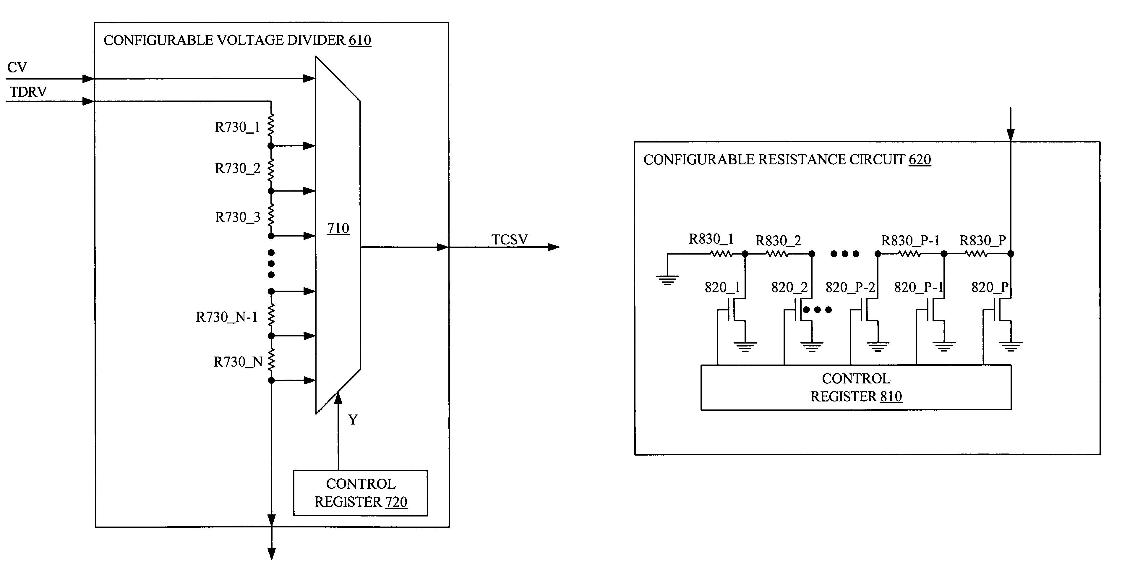
[0024]As explained above, propagation delay of buffer stages vary with temperature. The present invention compensates for temperature variations by adjusting the supply voltage to the buffer stage in response to temperature fluctuations. Specifically, the propagation delay of a buffer stage is inversely proportional with the supply voltage provided to the transistor. Thus, increasing the supply voltage decreases the propagation delay; and decreasing the supply voltage increases the propagation delay. The principles of the present invention may also be applied to other logic circuits, such as buffers, inverters, AND gates, NAND gates, OR gates, NOR gates, XOR gates, and XNOR gates, to compensate for temperature variations.
[0025]FIG. 4 is a block diagram of a temperature compensated voltage supply 400 in accordance with one embodiment of the present invention. Temperature compensated voltage supply 400 includes a reference voltage circuit 410 and a configurable voltage bias circuit 42...
PUM
 Abstract
Description
Claims
Application Information
 - R&D
- Intellectual Property
- Life Sciences
- Materials
- Tech Scout
- Unparalleled Data Quality
- Higher Quality Content
- 60% Fewer Hallucinations
Browse by: Latest US Patents, China's latest patents, Technical Efficacy Thesaurus, Application Domain, Technology Topic, Popular Technical Reports.
© 2025 PatSnap. All rights reserved.Legal|Privacy policy|Modern Slavery Act Transparency Statement|Sitemap|About US| Contact US: help@patsnap.com


