Apparatus and method for cleaning a semiconductor wafer

a technology for cleaning apparatus and semiconductor wafers, applied in the direction of cleaning using tools, cleaning using liquids, chemistry apparatus and processes, etc., can solve the problems of damage to patterns, lifting patterns, and damage to patterns

Inactive Publication Date: 2006-08-15
SAMSUNG ELECTRONICS CO LTD
View PDF4 Cites 2 Cited by
  • Summary
  • Abstract
  • Description
  • Claims
  • Application Information

AI Technical Summary

Benefits of technology

[0007]At least one exemplary embodiment of the present invention provides an apparatus for cleaning a semiconductor wafer that uses high frequency acoustic energy to clean the wafer. The apparatus includes an energy concentration relieving member that is positioned a distance from the semiconductor wafer to be cleaned. The energy concentration relieving member is formed at a height that is substantially equivalent to (e.g., co-planar to) the surface of the wafer. A probe is positioned substantially parallel to and over at least a portion of the energy concentration relieving member and a portion of the semiconductor wafer. The probe can be formed of a material that is non-reactive compared to solutions used to clean the semiconductor wafer and which easily transmits acoustic energy.
[0011]At least one other exemplary embodiment of the present invention provides a method for cleaning a semiconductor wafer. An energy concentration relieving member is positioned adjacent to and a distance from the semiconductor wafer to be cleaned. The energy concentration relieving member can be positioned at substantially the same height as, and substantially co-planar to, the semiconductor wafer to create a false edge for the semiconductor wafer. The false edge can shift the maximum acoustic power to the energy concentration relieving member.
[0014]Once the cleaning medium layer is formed over the semiconductor wafer and at least a portion of the energy concentration relieving member, voltage is applied to the vibrator and acoustic waves are generated by the vibrator. These acoustic waves are transferred to the probe, through the cleaning medium layer, and to the semiconductor wafer. The semiconductor wafer can be independently rotated about a rotation axis to ensure that the entire semiconductor wafer is vibrated by the probe. The acoustic energy transmitted to the surface of the semiconductor wafer by the vibrations of the probe removes pollutants and / or unwanted debris from the semiconductor wafer.

Problems solved by technology

Damage to the patterns includes, for example, lifting of the patterns.
In particular, patterns can be severely damaged on the edge of the wafer.
It is known that damage to the patterns occurs due to a concentration of megasonic energy or vibrational energy of fluids.
As design rules required for a semiconductor device become more narrow, damage to the patterns can increase.
For example, if a line width of the pattern is less than 0.12 μm, damage to the patterns due to the cleaning process can increase.

Method used


Image

  • Apparatus and method for cleaning a semiconductor wafer
  • Apparatus and method for cleaning a semiconductor wafer
  • Apparatus and method for cleaning a semiconductor wafer

Examples


Embodiment Construction

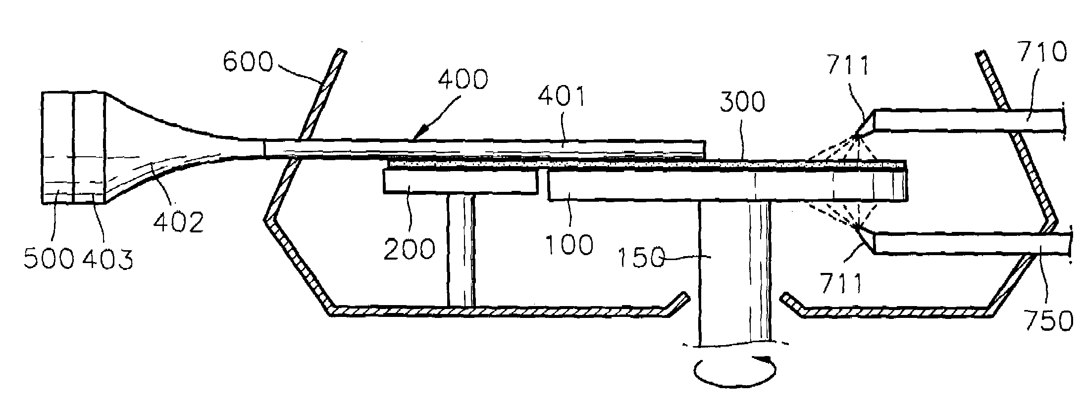
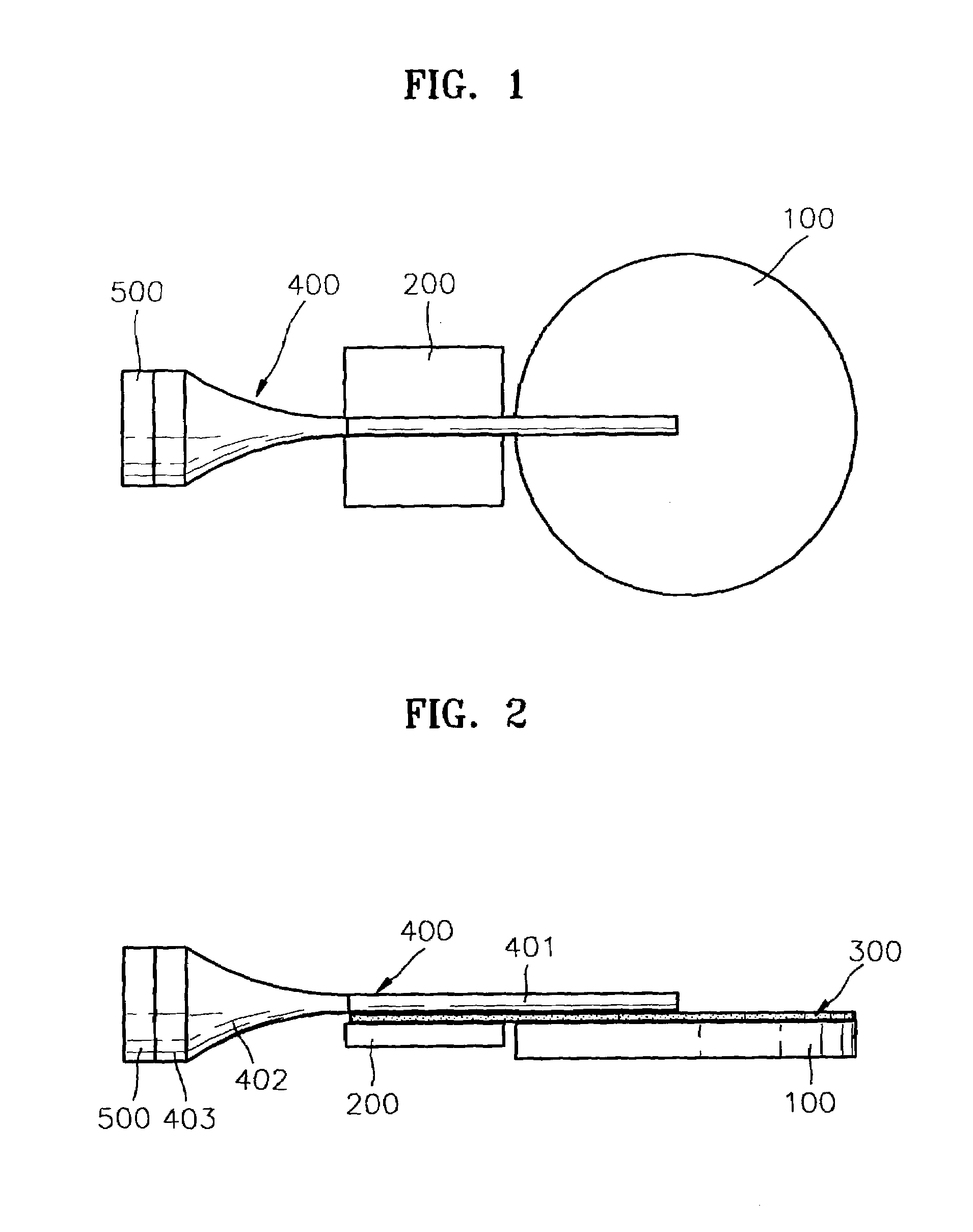
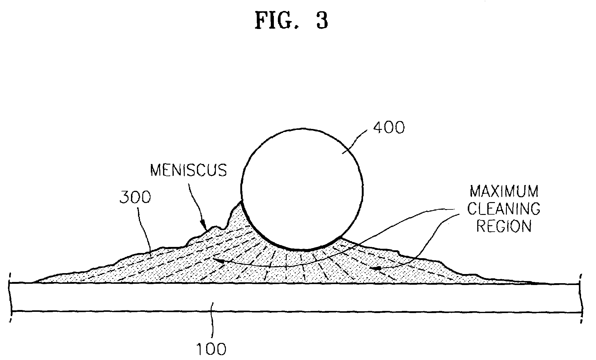
[0022]Exemplary embodiments of the present invention now will be described more fully below with reference to the accompanying drawings, in which exemplary embodiments of the invention are shown. The invention may, however, be embodied in many different forms and should not be construed as being limited to the exemplary embodiments set forth herein. Rather, these exemplary embodiments are provided so that this disclosure will be thorough and complete, and will fully convey the concepts of the present invention to those skilled in the art. In the drawings, the thickness of layers and regions are exaggerated for clarity. Like reference numerals in different drawings refer to like elements. Also, when it is written that a component or layer is formed “on” another component or layer, the component or layer can be formed directly on the other component or layer, or other components or layers can intervene therebetween.

[0023]A general description of a cleaning apparatus for cleaning a sem...


PUM

PropertyMeasurementUnit
widthaaaaaaaaaa
frequencyaaaaaaaaaa
energy concentrationaaaaaaaaaa

Abstract

The apparatus for cleaning a wafer includes an energy concentration relieving member positioned at the side of the wafer. An elongated portion of a probe extends over and substantially parallel to the wafer surface. A vibrator is attached to a rear end of the probe for vibrating the probe such that the elongated portion transfers acoustic vibrational energy to the wafer and dislodges debris.

Description

CROSS REFERENCE TO RELATED APPLICATIONS[0001]This U.S. nonprovisional application claims priority under 35 U.S.C. § 119 to Korean Patent Application No. 2002-20470 filed Apr. 15, 2002, the contents of which are incorporated by reference in its entirety.BACKGROUND OF THE INVENTION[0002]1. Field of the Invention[0003]The present invention relates to an apparatus and method for cleaning a wafer used in the manufacture of a semiconductor device.[0004]2. Description of the Related Art[0005]Recently, numerous methods for cleaning a wafer using high frequency acoustic energy, such as megasonic energy, have been introduced. An apparatus for cleaning a semiconductor wafer using megasonic energy removes pollutants (e.g., particles) from a wafer surface by providing megasonic energy through the cleaning fluid. One example of an apparatus for cleaning a semiconductor wafer that uses high frequency acoustic energy is the GOLD FINGER cleaning apparatus introduced by Verteq, Inc., which is disclos...

Claims


Application Information

Patent Timeline
Patent Type & Authority Patents(United States)
IPC IPC(8): B08B6/00H01L21/683B08B3/12C25F1/00H01L21/00H01L21/302H01L21/304H01L21/68
CPCB08B3/12H01L21/67051Y10S134/902H01L21/304
Inventor YEO, IN-JUNYOON, BYOUNG-MOONKIM, KYUNG-HYUNHAH, SANG-ROKNAM, JEONG-LIMJO, HYUN-HO
Owner SAMSUNG ELECTRONICS CO LTD
Why Eureka
Try Eureka