Electronic device, production method thereof, and plasma process apparatus

a technology of plasma process and electronic device, which is applied in the direction of electric discharge tubes, chemical vapor deposition coatings, coatings, etc., can solve the problems of insufficient difficult to achieve sufficient dissociation of source gas and form a high quality thin film on the target substrate, etc., to achieve the effect of improving the accuracy of the plasma process and increasing the quality of the produced electronic device or the lik

Inactive Publication Date: 2006-08-15
SHARP KK
View PDF4 Cites 25 Cited by
  • Summary
  • Abstract
  • Description
  • Claims
  • Application Information

AI Technical Summary

Benefits of technology

[0041]In a plasma process apparatus of the present invention, decomposition and dissociation of a gas with plasma is accelerated even at a low target substrate temperature while suppressing plasma damage to a surface on which a film is to be formed. Thus, the accuracy of the plasma process is improved, and the quality of a produced electronic device, or the like, is increased.

Problems solved by technology

Conventionally established plasma CVD apparatuses possess various limitations.
When the conventional CVD apparatus is used in the production of a large surface electronic device, such as a liquid crystal display, an amorphous solar cell device, or the like, it is sometimes difficult to achieve sufficient dissociation of the source gas and form a high quality thin film on the target substrate 4.
For example, in a conventionally known parallel plate type apparatus, dissociation of the source gas is sometimes insufficient.
However, for example, in the case where the silicon nitride film is formed on a copper wiring, there is a possibility that ammonium gas corrodes the copper.
In such a case, the parallel plate type apparatus cannot sufficiently decompose hydrogen gas and nitrogen gas, which are unlikely to be dissociated, and therefore, it is difficult to obtain a silicon nitride film having desirable insulating film characteristics and protection film characteristics.
That is, it is understood that, also in this case, the parallel plate type apparatus cannot sufficiently accelerate dissociation of the source gas.
However, this plasma apparatus also cannot accelerate dissociation of the source gas.
However, in this apparatus, the surface of the target substrate is exposed to the plasma so that a surface of the substrate on which a film is formed is subjected to plasma damage.
However, when the temperature of the target substrate 4 is set to 200° C. or lower, a desirable film quality cannot be maintained.
That is, a method for forming a high quality film by a plasma CVD apparatus with high gas dissociation efficiency especially at a low target substrate temperature has not yet been established.
That is, a high performance plasma process apparatus which operates with high gas dissociation efficiency has not yet been established.
The thin films formed using the above techniques do not have sufficient protection film characteristics for use as devices.
However, in the conventional plasma CVD apparatuses, a protection film having a desirable quality is not formed with such a temperature condition.
For example, Applied Physics Letters, volume 65, pages 2229–2231 reports that, in the case where a silicon nitride film is formed as a protection film at 100° C., the quality of the silicon nitride film is poor so that water vapor contained in the atmosphere penetrates into the film, and silicon and oxygen are bonded.
In a currently employed production method, another glass substrate is sealingly attached as a cap over the device in a nitrogen atmosphere for separation from the atmosphere because the quality of the protection film is poor.
These devices also suffer from the above described quality problems.

Method used


Image

  • Electronic device, production method thereof, and plasma process apparatus
  • Electronic device, production method thereof, and plasma process apparatus
  • Electronic device, production method thereof, and plasma process apparatus

Examples


embodiment 1

[0077](Embodiment 1)

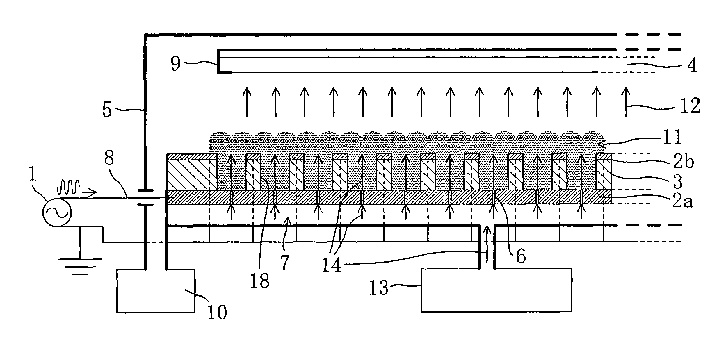
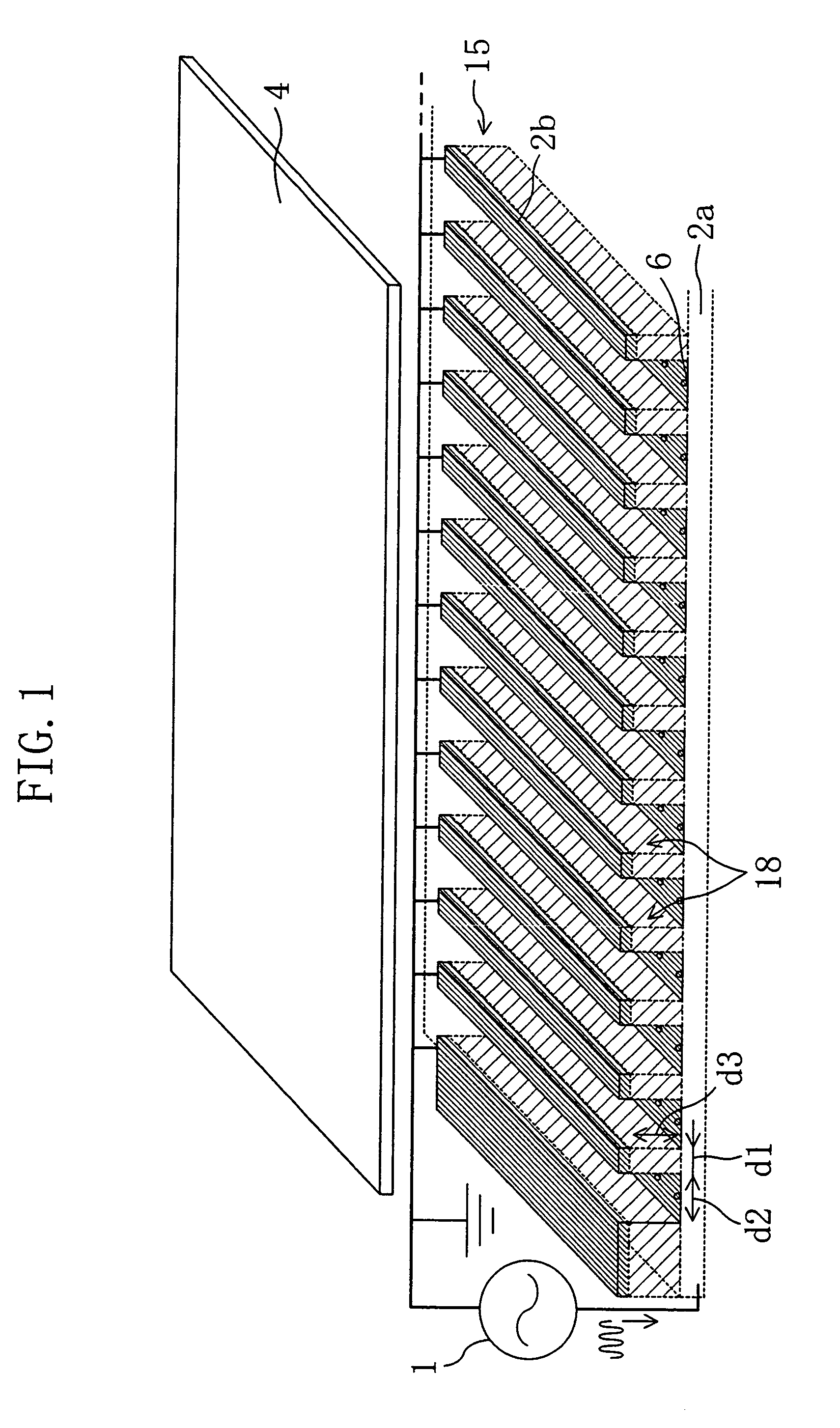
[0078]The structure of a plasma CVD apparatus according to embodiment 1 of the present invention is described with reference to FIGS. 1 and 2. FIG. 1 is a perspective view schematically showing the plasma CVD apparatus of embodiment 1. FIG. 2 is a cross-sectional view schematically showing the plasma CVD apparatus of embodiment 1.

[0079]The plasma CVD apparatus includes a process chamber (vacuum container) 5 in which a substrate 4 to be processed (target substrate 4) is installed, gas inlets 6 through which a source gas is introduced into the process chamber 5, and a plasma discharge production section 15 provided in the process chamber 5. Typically, a substrate holder 9 for holding the target substrate 4 is provided in the process chamber 5, and the target substrate 4 is placed on the substrate holder 9. Moreover, the substrate holder 9 can apply a bias voltage to the target substrate 4 as necessary by using a DC power supply or a low frequency power supply.

[0080...

embodiment 2

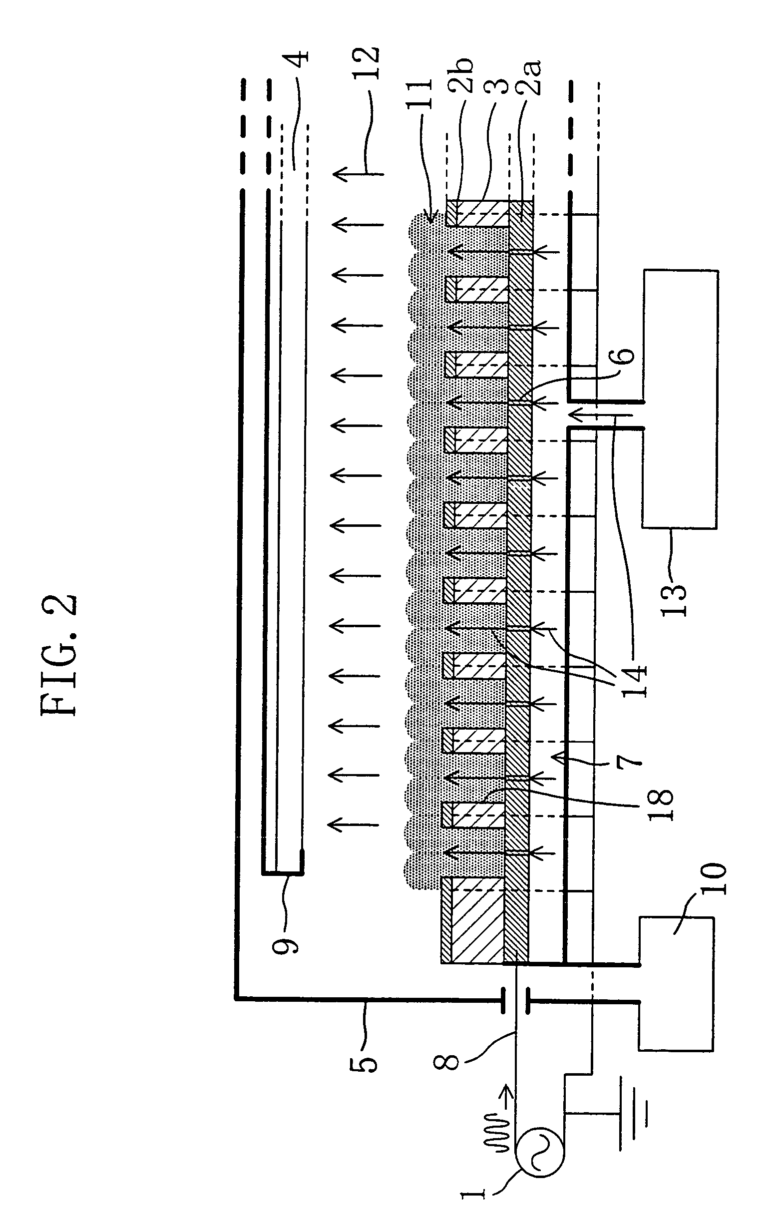
[0120](Embodiment 2)

[0121]FIG. 6 is a perspective view schematically showing a plasma CVD apparatus according to embodiment 2 of the present invention. FIG. 7 is a cross-sectional view schematically showing the plasma CVD apparatus of embodiment 2. FIG. 8 is an enlarged cross-sectional view showing a part of the apparatus of FIG. 7. The plasma CVD apparatus of embodiment 2 is described with reference to FIGS. 6 through 8. In the following descriptions, components having substantially the same functions as those of the components of the plasma CVD of embodiment 1 are denoted by the same reference numerals used in embodiment 1, and descriptions thereof are herein omitted.

[0122]The plasma CVD apparatus of embodiment 2 is different from the plasma CVD of embodiment 1. In the apparatus of embodiment 2, the plasma discharge surface of the cathode electrode 2a includes a concaved surface, whereas in the apparatus of embodiment 1, the plasma discharge surface of the cathode electrode 2a is ...

embodiment 3

[0135](Embodiment 3)

[0136]An organic electroluminescence device, which is an electronic device actually fabricated using the plasma CVD apparatus of embodiment 1 or 2, is described below. FIG. 9 is a cross-sectional view schematically showing an organic electroluminescence device.

[0137]The electroluminescence device (hereinafter, simply referred to as “EL device”) shown in FIG. 9 includes an anode 26 made of aluminum, an organic hole transport layer 25, an organic emission layer 24, a cathode 23 made of calcium, and a transparent electrode 22 made of indium tin oxide, which were formed on the target substrate 4 in this order. The films of the organic hole transport layer 25 and the organic emission layer 24 were formed of a diamine derivative ((1,1′-bis(4-di-p-tolylaminophenyl)cyclohexane; TPD) and 8-quinolinol aluminum complex (tris(8-hydroxyquinolinato)aluminum(III);Alq3), respectively, by using a vacuum deposition method.

[0138]The organic EL device of embodiment 3 further include...


PUM

PropertyMeasurementUnit
frequencyaaaaaaaaaa
frequencyaaaaaaaaaa
frequencyaaaaaaaaaa

Abstract

A plasma process apparatus for performing a plasma process on a target substrate 4 includes a process chamber 5 in which the target substrate 4 is installed, a gas inlet 6 for introducing a gas into the process chamber 5, and a plasma discharge production section 15 provided in the process chamber 5. The plasma discharge production section 15 includes a first electrode 2a and a second electrode 2b that is closer to the target substrate 4 than the first electrode 2a is. Only surfaces of the first electrode 2a and the second electrode 2b which can be seen in the normal line direction of the target substrate 4 function as plasma discharge surfaces. Thus, a high quality film is realized even at a low target substrate temperature, and the film formation is performed with high gas dissociation efficiency.

Description

BACKGROUND OF THE INVENTION[0001]1. Field of the Invention[0002]The present invention relates to an electronic device having functionality and to a production method of the electronic device. Specifically, the present invention relates to an electronic device including a semiconductor film, an organic film, an insulating film, etc., and to a production method of the electronic device. Further, the present invention relates to a plasma process apparatus for forming a thin film of semiconductor, conductor, or the like. Specifically, the present invention relates to plasma process apparatuses, such as a plasma chemical vapor deposition apparatus using a plasma-activated chemical vapor deposition method, which is used for forming a thin film of semiconductor, conductor, or the like, a dry etching apparatus used for forming a thin film pattern of a semiconductor film or conductor film, and an asher apparatus for removing a resist used in the formation of a thin film pattern.[0003]2. Desc...

Claims


Application Information

Patent Timeline
Patent Type & Authority Patents(United States)
IPC IPC(8): H01L21/00H01L21/64C23C16/509H01L21/3065H01J37/32
CPCC23C16/5096H01J37/32009H01J37/32532H01J37/32082Y10T29/41H01L21/3065
Inventor MIYAZAKI, ATSUSHIHATANO, AKITSUGUSAKAI, OSAMU
Owner SHARP KK
Why Eureka
Try Eureka