Method for nitriding substrate and method for forming insulating film

a technology of nitriding substrate and insulating film, which is applied in the direction of coating, solid-state device, chemical vapor deposition coating, etc., can solve the problems of deteriorating quality of silicon nitride film, damage to silicon substrate, and deterioration of nitride film quality, so as to improve film quality and improve the effect of electron temperature and ion energy, the effect of reducing the damage to the substra

Inactive Publication Date: 2010-10-26
TOKYO ELECTRON LTD
View PDF9 Cites 4 Cited by
  • Summary
  • Abstract
  • Description
  • Claims
  • Application Information

AI Technical Summary

Benefits of technology

[0031]In accordance with the present invention, the silicon is directly nitrided using the nitrogen-containing plasma by controlling the sheath voltage Vdc to be less than or equal to about 3.5 eV, thus suppressing a plasma damage and forming a thin silicon nitride film having high-quality.
[0033]By controlling the sheath voltage Vdc to be in a range from 0 to 2 eV, the N concentration of the silicon nitride film can be further increased and the film quality can be further improved.
[0034]Further, by forming the nitrogen-containing plasma by introducing the microwave into the processing chamber via the planar antenna member having a plurality of slots, the electron temperature and the ion energy of the plasma can be further decreased, and hence, the plasma damage on the substrate can be decreased further.
[0035]Moreover, by disposing the dielectric plate having a plurality of through holes between the plasma generating region and the target substrate in the processing chamber, the control of the sheath voltage Vdc can be performed readily. In this case, by setting the processing pressure to be in a range from 6.8 Pa to 1333 Pa and the processing temperature to be in a range from 600 to 900° C. as well as using the dielectric plate, the sheath voltage Vdc can be more readily adjusted to a desired value. That is, by combining the hardware configuration of the plasma processing apparatus and the process conditions, the sheath voltage Vdc can be controlled more delicately and also more readily.

Problems solved by technology

Further, though a method of directly nitriding the silicon substrate by forming a plasma of the ammonia gas with a parallel plate type plasma processing apparatus is also disclosed in Reference 2, there occurs a problem in such case that a damage of the silicon substrate is caused due to a very high energy of the plasma or a quality of the silicon nitride film deteriorates due to an unexpected reaction.
As pointed out in Reference 2, when a nitride film is formed by directly nitriding silicon by the plasma, there may be incurred a so-called plasma damage that the quality of the nitride film deteriorates due to an implantation of high-energy ions into the film.
This plasma damage would have an adverse influence upon characteristics of a device, e.g., a transistor, resulting in deterioration of device performance.
Further, when the silicon is plasma-nitrided directly, there is a problem that an N concentration decreases (N is lost from the film) or oxidation readily occurs with a lapse of time.
In particular, as the thickness of the nitride film decreases, the possibility of the film quality deterioration due to the N loss or the oxidation increases.
Thus, a formation of a stable nitride film becomes difficult.

Method used


Image

  • Method for nitriding substrate and method for forming insulating film
  • Method for nitriding substrate and method for forming insulating film
  • Method for nitriding substrate and method for forming insulating film

Examples


Embodiment Construction

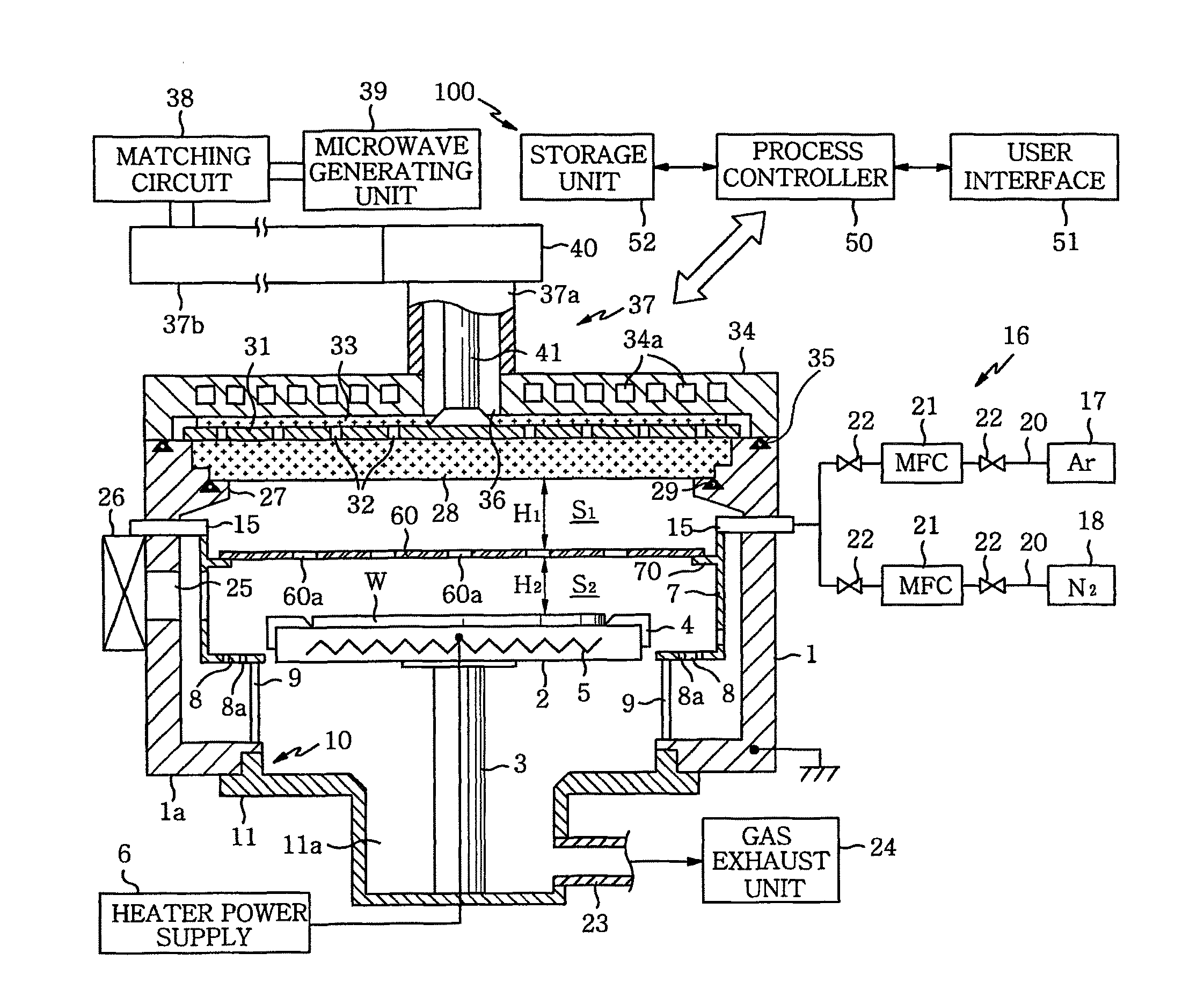
[0056]Hereinafter, embodiments of the present invention will be described in detail with reference to the accompanying drawings. FIG. 1 is a cross sectional view schematically showing an exemplary plasma processing apparatus which is preferably applicable to the present invention. The plasma processing apparatus 100 is configured as an RLSA (Radial Line Slot Antenna) microwave plasma processing apparatus capable of generating a high-density microwave plasma having a low electron temperature by way of generating the plasma while introducing a microwave into a processing chamber via a planar antenna having a plurality of slots, especially, an RLSA antenna. With this plasma processing apparatus 100, a desired process can be performed by a plasma having a density of about 1×10¹⁰ to 5×10¹⁰ / cm3 and an electron temperature of about 0.7 to 2 eV.

[0057]Therefore, this plasma processing apparatus 100 can be preferably employed in a manufacturing process of various semiconductor devices such as...


PUM

PropertyMeasurementUnit
sheath voltage Vdcaaaaaaaaaa
diametersaaaaaaaaaa
pressureaaaaaaaaaa

Abstract

In a substrate nitriding method for nitriding a target substrate by allowing a nitrogen-containing plasma to act on silicon on a surface of the substrate in a processing chamber of a plasma processing apparatus, the nitridation by the nitrogen-containing plasma is performed by controlling a sheath voltage Vdc around the substrate to be less than or equal to about 3.5 eV. The sheath voltage Vdc is a potential difference Vp−Vf between a plasma potential Vp in a plasma generating region and a floating potential Vf of the substrate.

Description

FIELD OF THE INVENTION[0001]The present invention relates to a substrate nitriding method and an insulating film forming method for processing a target substrate such as a semiconductor wafer by using a plasma to thereby form a silicon nitride film on the target substrate.BACKGROUND OF THE INVENTION[0002]In a manufacturing process of various semiconductor devices, a silicon nitride film is formed as a gate insulating film of, e.g., a transistor. As a method for forming the silicon nitride film, there is proposed, e.g., a method for forming a silicon oxynitride film by introducing nitrogen into a silicon oxide film by a plasma process, in addition to a method for depositing a silicon nitride film by CVD (Chemical Vapor Deposition) (see, for example, Reference 1).[0003]Meanwhile, with the recent trend of miniaturization of semiconductor devices, a gate insulating film is getting thinner, and it is required to form a thin gate insulating film having a film thickness of several nanomete...

Claims


Application Information

Patent Timeline
Patent Type & Authority Patents(United States)
IPC IPC(8): H01L21/318
CPCH01L21/28202H01L21/3185H01L29/518H01J2237/3387H01L21/3211H01L2924/0002H01L2924/00H01L21/02247H01L21/02252H01L21/0217
Inventor HONDA, MINORUNAKANISHI, TOSHIO
Owner TOKYO ELECTRON LTD
Why Eureka
Try Eureka