[0005]Therefore a need has arisen for a method and
system which improves ALD thin film quality.
[0007]In accordance with the present invention, a method and
system are provided that substantially eliminates or reduces disadvantages and problems associated with previously developed methods and systems for ALD. Periodic annealing during ALD of thin films after a predetermined film thickness or associated number of deposition cycles improves film quality.
Throughput is improved by maintaining desired process parameters for precursor flow, reactant flow and purge cycles, with reduced
cycle time and risk of introducing impurities accomplished with a dual zone showerhead to limit mixing of residual reactants.
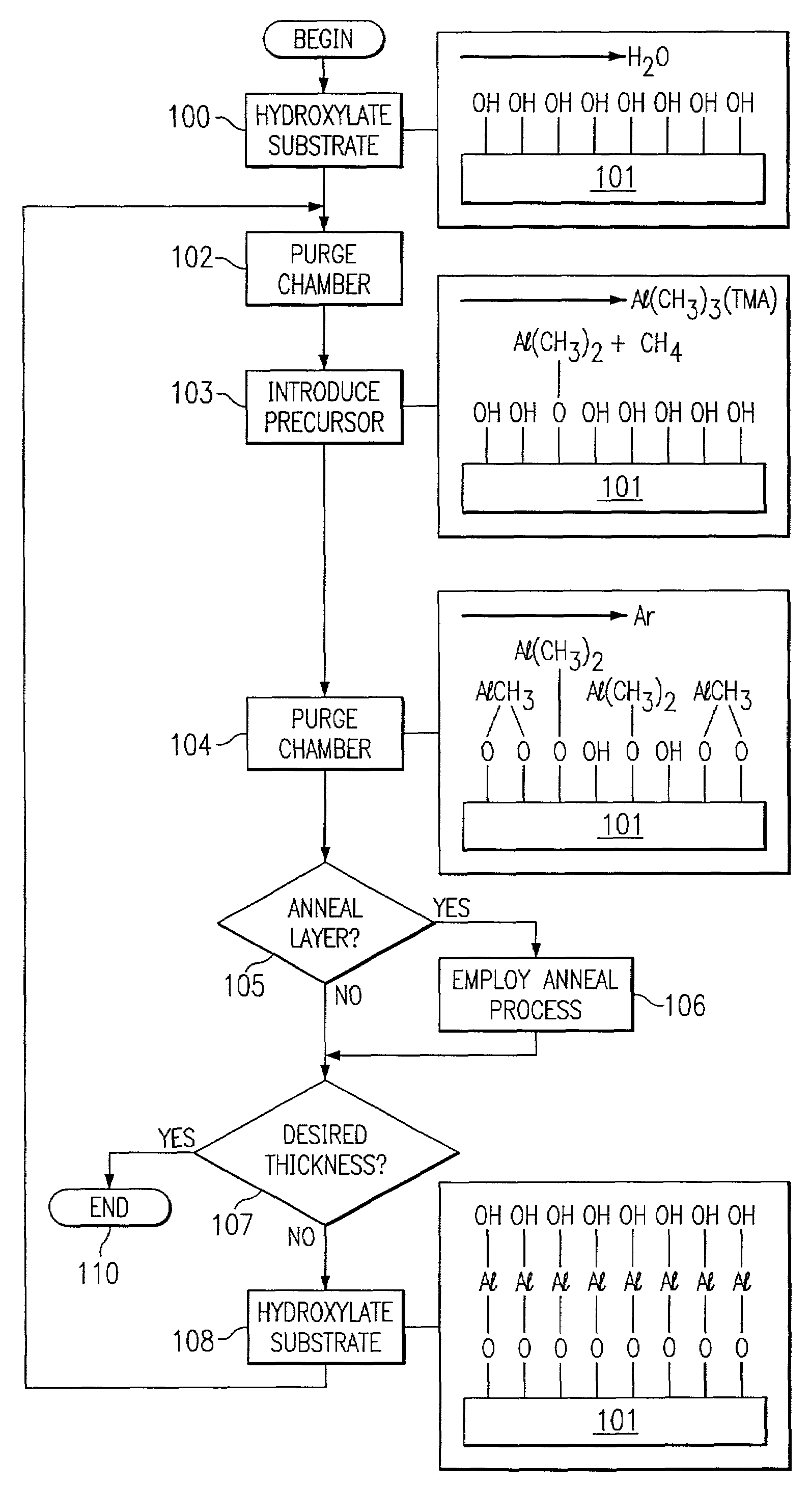
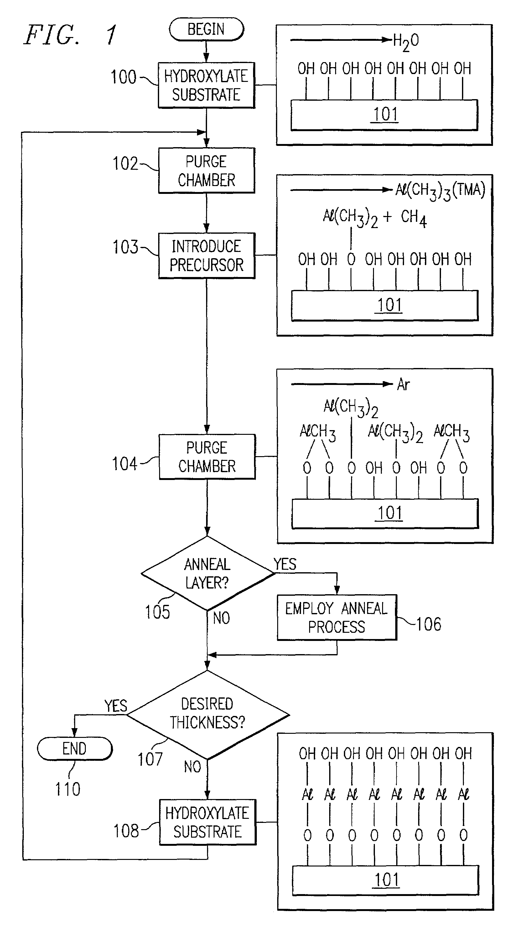
[0008]More specifically, a method of fabricating a conformal thin film for integrated electronic structures is provided. ALD cycles of adsorbing and reacting a precursor on a wafer to deposit the thin film are performed with intervening anneals to control the quality of the ALD film. Process
throughput and quality are enhanced by the use of a dual zone showerhead and by control of predetermined process parameters, such as precursor and reactant flow times and quantity, purge times, the number and frequency of anneals, and wafer temperature, so that contaminants are reduced and film breakdown
field strength and intrinsic stress are at desired levels.
[0009]In one embodiment of the present invention, an aluminum
oxide thin film is deposited with a predetermined number of ALD cycles and with one or more intervening anneals performed after a predetermined number of ALD cycles or associated number film thickness. An ALD cycle comprises distributing a precursor through a first zone of a multi-zone
shower head to achieve a continuous
monolayer of precursor adsorption on the wafer, and purging the
processing chamber. The
monolayer of precursor is oxidized with a flow of water through a second zone of the multi-zone showerhead, and the
processing chamber purged to prepare for another ALD cycle. The wafer is maintained at a generally low temperature of between 60 and 350 C to aid in the adsorption of a continuous monolayer of precursor that is not thermally dissociated. Every 25–50 Å of film thickness, which at 0.8 Å per ALD cycle takes approximately 25 to 50 ALD cycles, a thermal or
plasma anneal of the ALD film is performed in a reactive ambient to reduce
impurity incorporation that generally results from lower wafer temperatures that leave the
chemical reaction between the precursor and reaction gas incomplete. For instance, by varying the frequency of an in-situ RF
plasma anneal in an Ar / O2 ambient, the intrinsic film stress of the AlOX film can be varied from tensile to compressive. The use of the multi-zone showerhead, predetermined precursor and reactant pulse times, and adequate purging increases throughput and reduces the introduction of contaminants to the wafer.
[0011]The present invention provides a number of important technical advantages. One important technical
advantage is that intrinsic stress is varied from tensile to compressive and
breakdown voltage for an ALD film is enhanced by varying the number of plasma anneals performed for a predetermined number of ALD cycles. For instance, a 60–200° C.
atomic layer deposition (ALD) process that provides smooth (Ra˜2 Å), pure (impurities <1 at. %), and highly conformal (100% step coverage) AlOx films with excellent
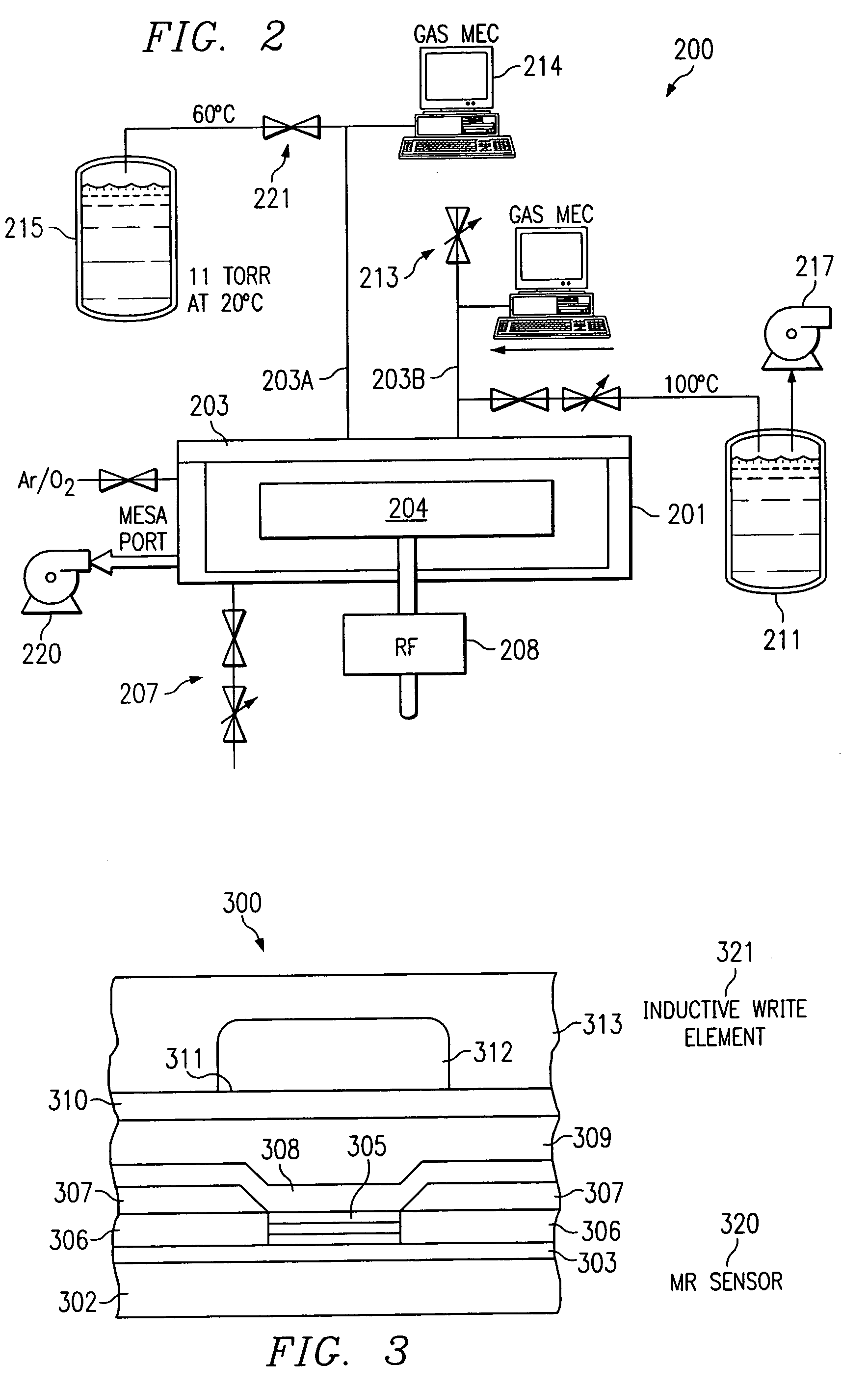
breakdown strength (9–10 MV / cm) is provided by performing a plasma anneal every 25 to 50 ALD cycles. In one form, optimal chamber configuration and precursor / oxidant
delivery methods have been identified for trimethylaluminum (TMA) as an aluminum source and water as an oxidant.
[0012]Another important technical
advantage is that the resulting ALD AlOx films are conformal and exhibit excellent insulating characteristics down to 5–10 Å to support thin film applications such as a gap layer for thin film heads or a
tunnel barrier for magnetic tunnel junctions.
Plasma annealing the films in-situ every 25–50 Å, makes the as-deposited tensile stress slightly compressive and the breakdown field to exceed 10 MV / cm. Advanced thin film heads for recording densities of 50 Gb / in2 and beyond require very thin and conformal gap layers. The process uses trimethylaluminum (TMA) as the aluminum source and water as the oxidant. Although ALD provides a relatively low
deposition rate, with proper
chamber design, commercial production throughput requirements can be met despite a relatively low
deposition rate of approximately 0.8 to 1.1 Å / cycle. A small chamber volume that allows a
cycle time of 5 s meets production throughput requirements of 4–6 wph for a 100 Å film.

