

Semiconductor device, semiconductor package, electronic device, electronic apparatus, and manufacturing methods of semiconductor device and electronic device
- Summary
- Abstract
- Description
- Claims
- Application Information
AI Technical Summary
Benefits of technology
Problems solved by technology
Method used
Image

Examples
Embodiment Construction
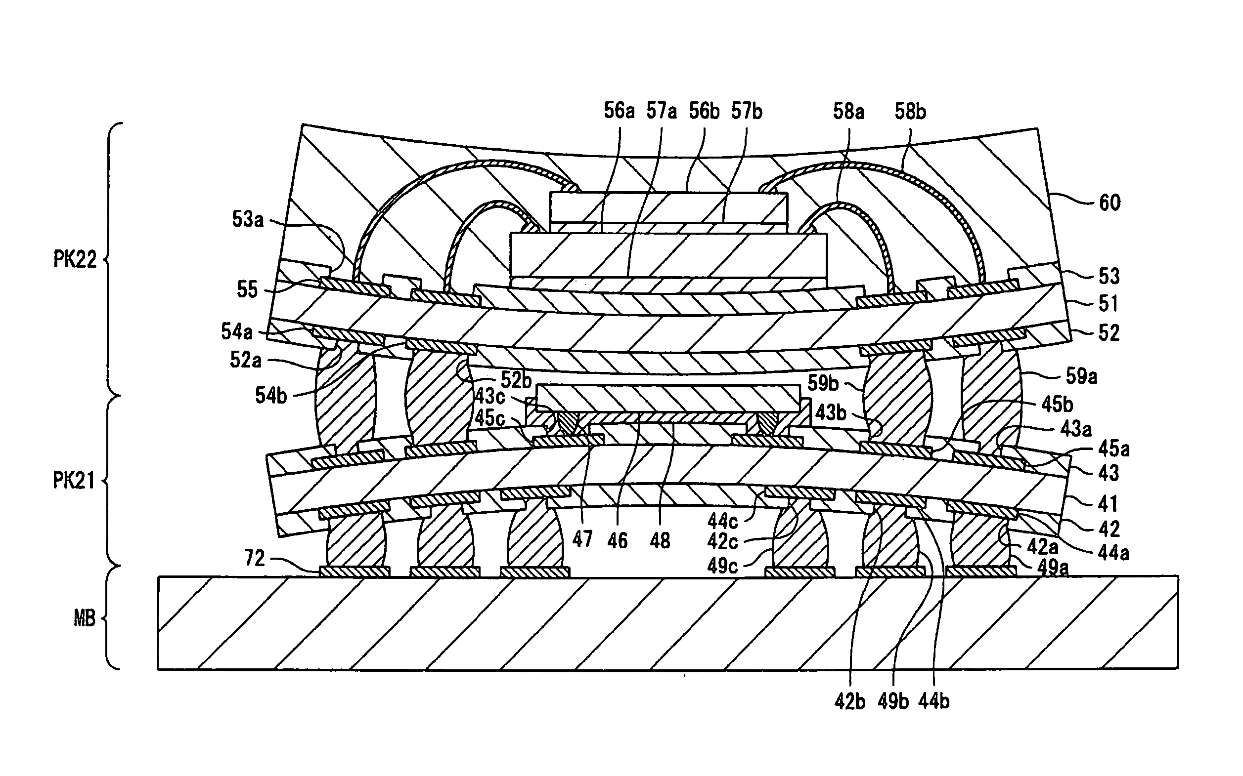
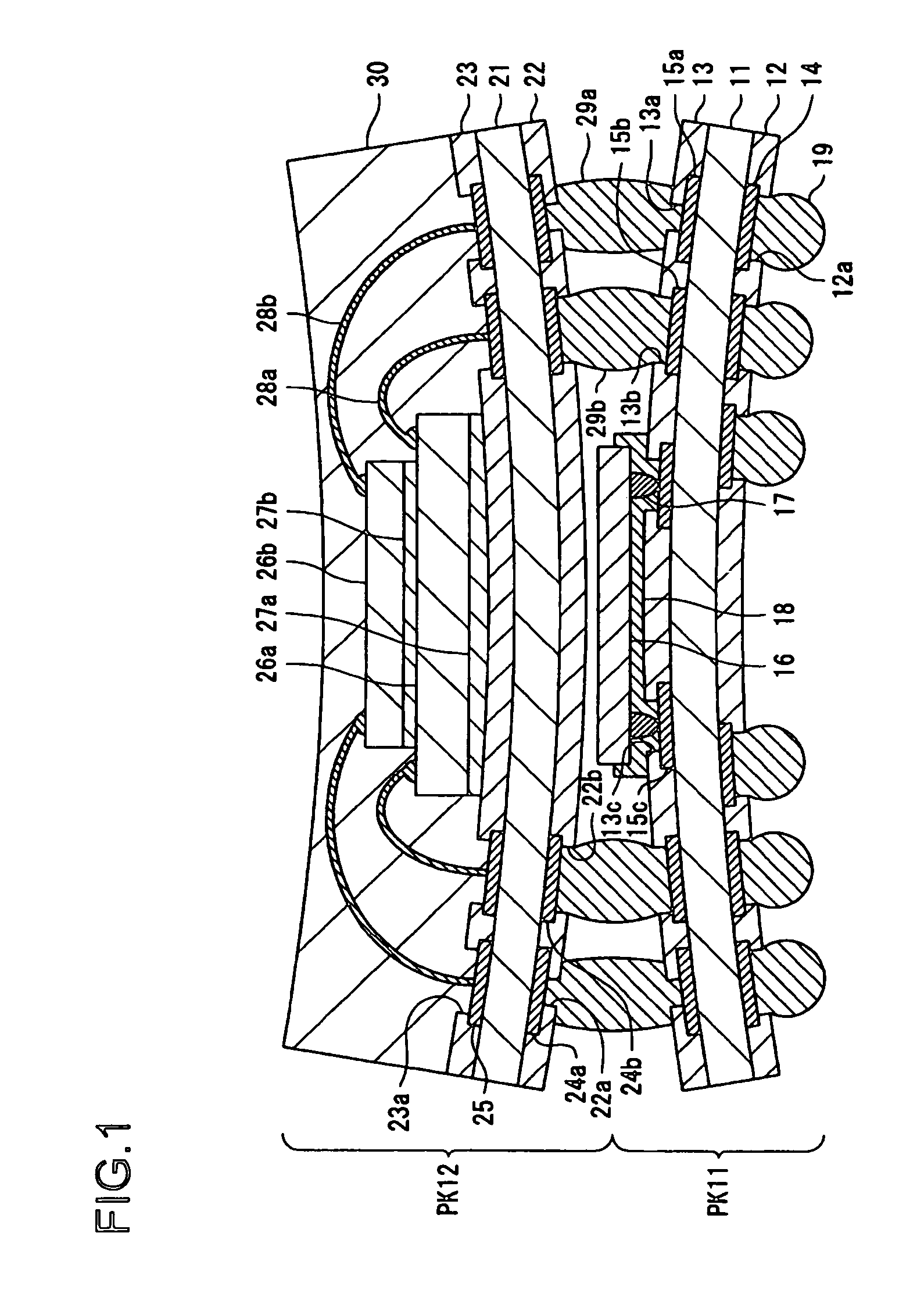
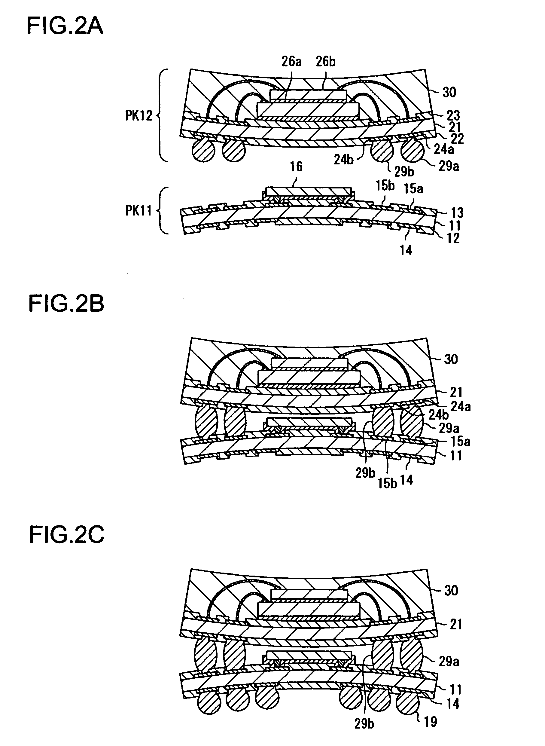
[0049]Hereinafter, a semiconductor device, an electronic device and a manufacturing method of the same according to embodiments of the present invention will be described referring to the drawings. FIG. 1 shows a cross-sectional view illustrating a constitution of a semiconductor device according to a first embodiment of the present invention. In the first embodiment, opening diameters of openings 13a and 13b and openings 22a and 22b for a semiconductor package PK11 and a semiconductor package PK12 respectively, with which protruding electrodes 29a and 29b are joined, are changed.
[0050]In FIG. 1, a carrier substrate 11 is provided in the semiconductor package PK11. On a back surface of the carrier substrate 11, lands 14 for arranging protruding electrodes 19 are provided. Furthermore, on the back surface of the carrier substrate 11 provided with the lands 14, an insulating layer 12 such as a solder resist is provided, and openings 12a for exposing surfaces of the lands 14 are provid...
PUM
 Abstract
Description
Claims
Application Information