

Double-sided chip on film packaging structure and manufacturing method thereof
- Summary
- Abstract
- Description
- Claims
- Application Information
AI Technical Summary
Benefits of technology
Problems solved by technology
Method used
Image

Examples
Embodiment Construction
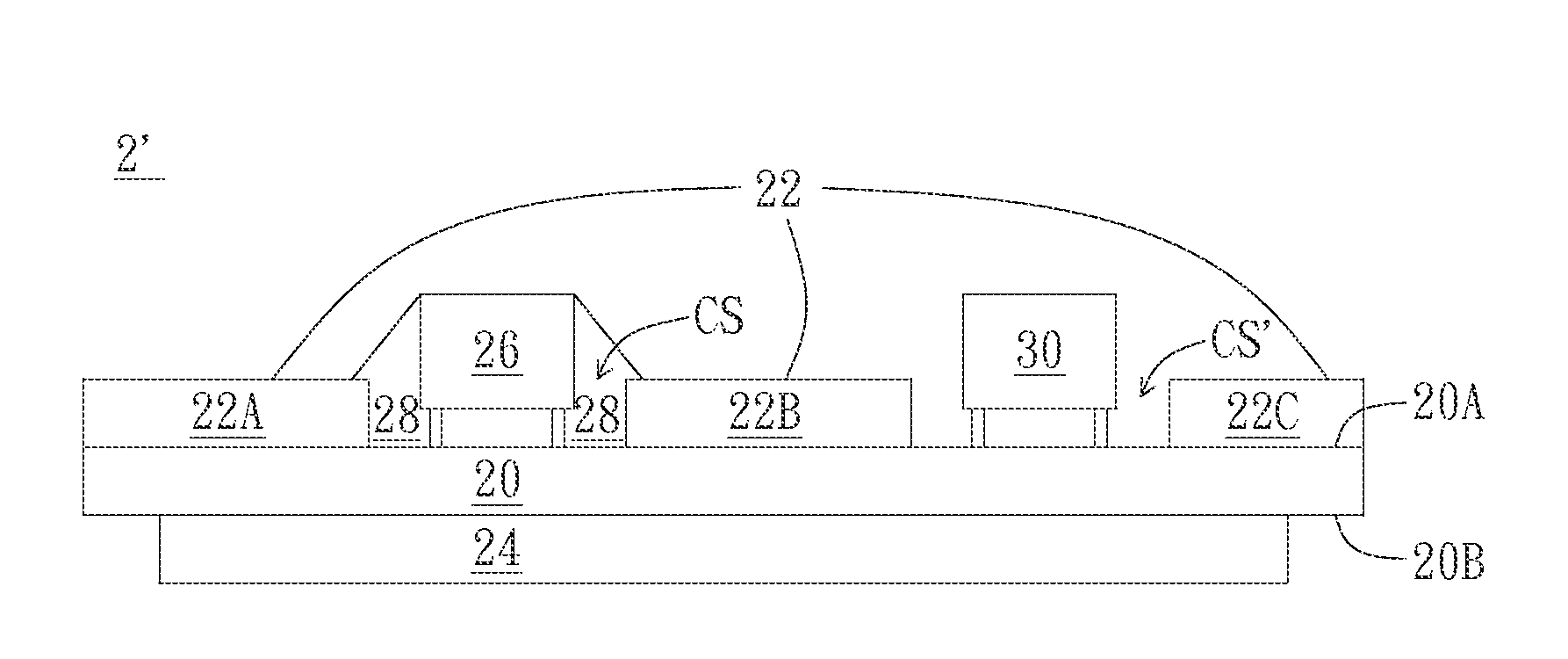
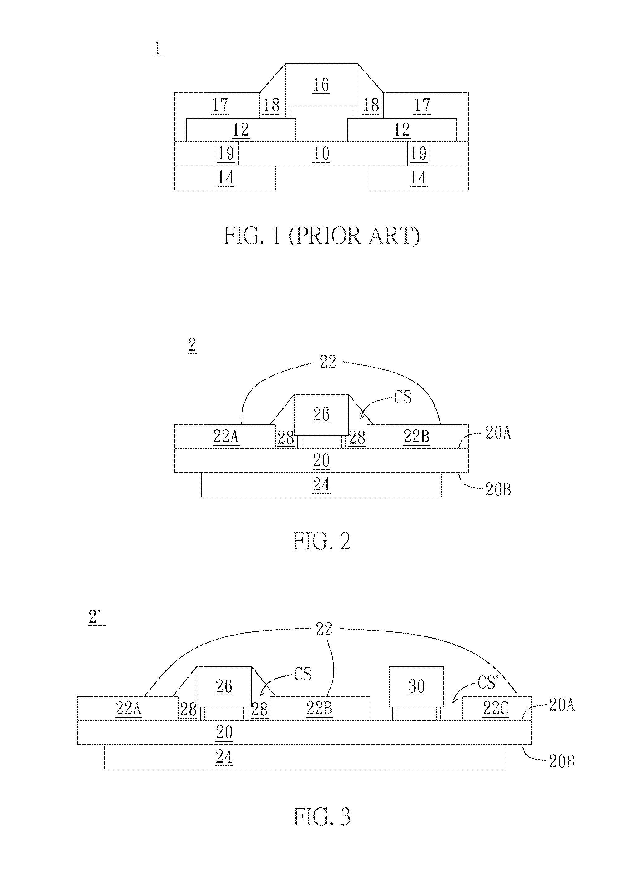
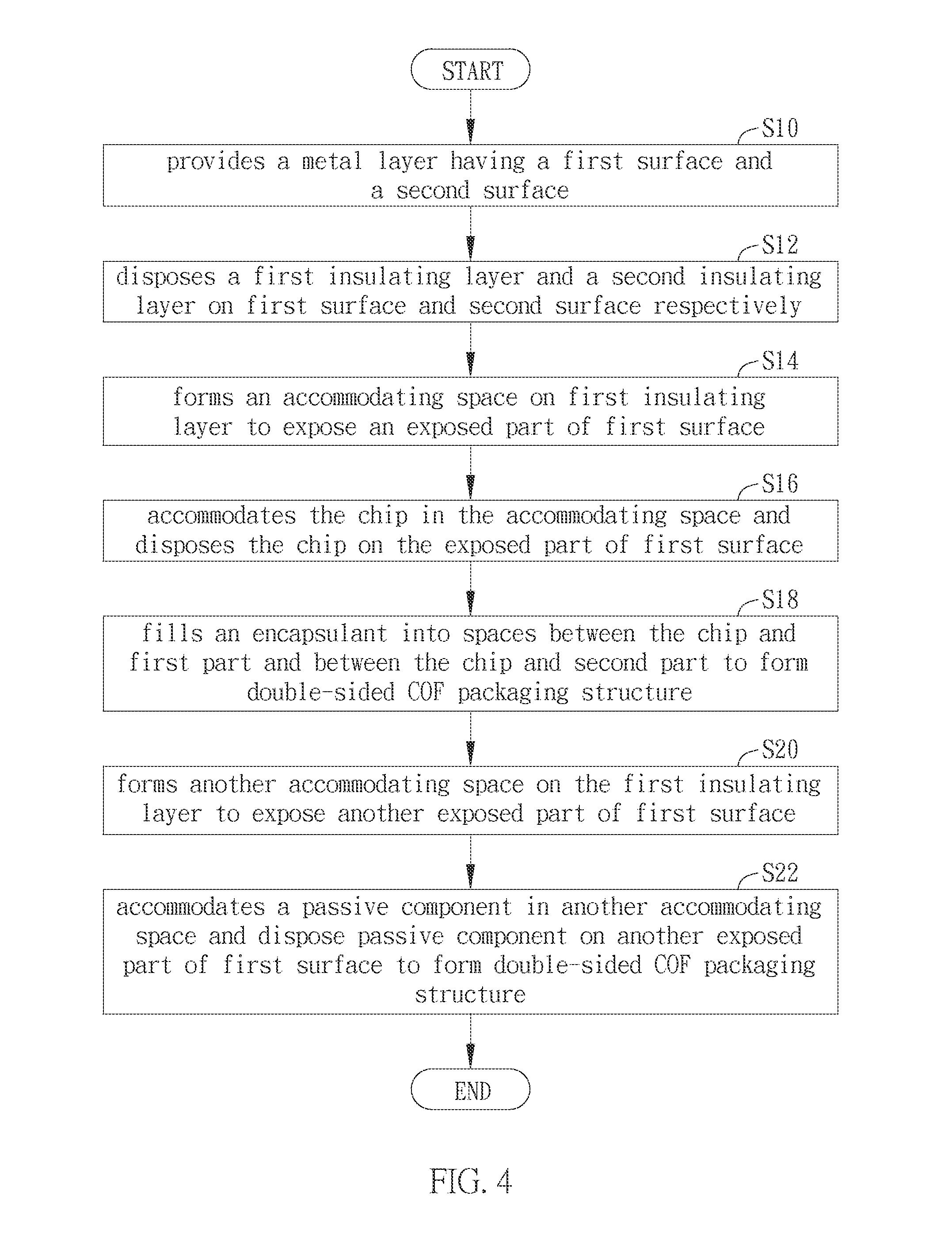
[0022]A preferred embodiment of the invention is a double-sided COF packaging structure. In this embodiment, the double-sided COF packaging structure is used to package a chip, and the chip can be a driving chip applied to a display apparatus, but not limited to this.
[0023]Please refer to FIG. 2. FIG. 2 illustrates a schematic diagram of the double-sided COF packaging structure in this embodiment. As shown in FIG. 2, the double-sided COF structure 2 at least includes a metal layer 20, a first insulating layer 22, a second insulating layer 24, a chip 26, and an encapsulant 28.
[0024]In this embodiment, the first insulating layer 22 and the second insulating layer 24 are disposed on a first surface 20A and a second surface 20B of the metal layer 20 respectively. The first surface 20A and the second surface 20B of the metal layer 20 are opposite; for example, the first surface 20A and the second surface 20B can be the upper surface and the lower surface of the metal layer 20 shown in FI...
PUM
 Abstract
Description
Claims
Application Information